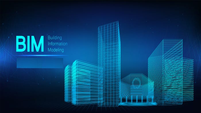
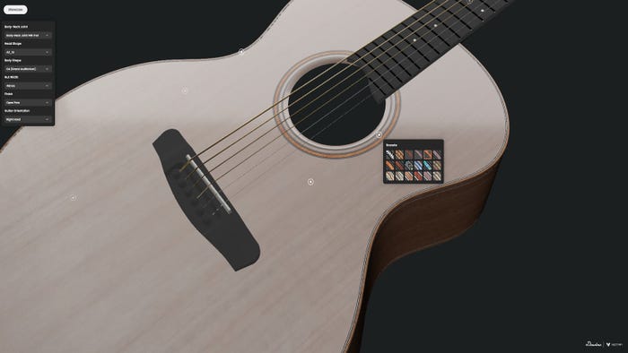
Design Software
CNC machining 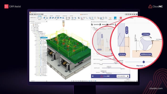
IndustryCatch These New AI Products and SystemsCatch These New AI Products and Systems
We’re looking at AI visual inspection, AI driven CNC machining, an AI analyzer, and more.


.jpg")


.jpg")


.jpg")


Editors' Choice


Jun 4 - Jun 6, 2024
Jun 4 - Jun 6, 2024
Innovation in automation starts here. Discover and collaborate on automation solutions that are revolutionizing the entire production lifecycle — from design to production to market — and sharpen your competitive edge. ATX South is part of IME South, a six-in-one expo offering the latest insights & solutions spanning medtech, packaging, automation, plastics, design, & processing.
Register NowSign up for the Design News Daily newsletter.