Use Virtual Twin Tech to Develop Semiconductors
Digital simulation has become a viable means to design next-gen ICs, ASICs, FPGAs, and other semiconductors. A Dassault Systemes executive explains how.

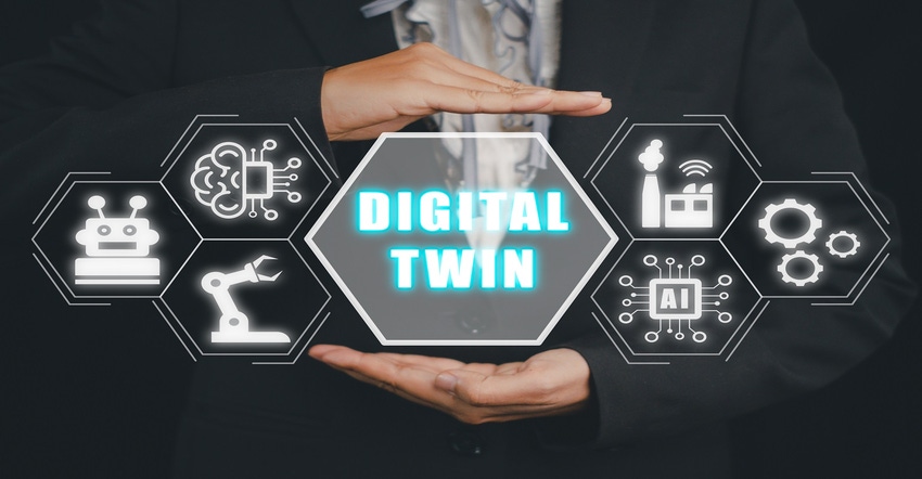
In recent years, the concept of using a digital virtual twin to develop a product or process has become popular, as companies seek a faster, more efficient means to get new technologies to market with less time-consuming, costly prototyping. Semiconductors, which have become increasingly complex devices, are a good candidate for virtual twin technology as design engineers can simulate the various physical and thermal characteristics of the parts, as well as the complex steps used to manufacture them.
In this e-mail interview, Manuel Rei, Semiconductor Industry Solution Experience Director, Dassault Systèmes, talks about how virtual twin technology is changing the process of designing semiconductors.
Design News: In using virtual twins to develop semiconductors, how accurate can simulations be in characterizing performance specs?
Manuel: Virtual twins are digital representations of physical products or systems that can be used for simulation, analysis, and optimization. In the context of semiconductor development, virtual twins can be extremely valuable in predicting and characterizing performance specifications.
The accuracy of virtual twin simulations in the context of semiconductor development depends on the complexity of the semiconductor’s design and the quality of the simulation models.
A more complex semiconductor design implies deeper and stronger connections between various components, such as transistors, dies, interconnects, and packages. Modeling and simulating these interactions on a platform where you can experiment the end-to-end device experience helps guarantee efficient time to market.
Design News: What aspects of semiconductor development are facilitated using virtual twin technology?
Manuel: Virtual twin technology can facilitate several aspects of semiconductor development, from new product introduction to end of life, including optimization and streamlining of the design, manufacturing, and testing processes.
Virtual twins can predict how different materials will behave in terms of conductivity and heat dissipation, from a molecular standpoint to the full device definition. Additionally, they can assist in selecting and characterizing materials for semiconductor components.
They can simulate manufacturing processes such as lithography, etching, and doping to help engineers optimize parameters for improved yield, performance, and reliability. Process variations can also be studied to understand their impact on final product specifications. Finally, comparing virtual simulation results to results obtained during manufacturing can help improve simulations.
Virtual twins can also accurately model and predict electrical and thermal behavior, and mechanical performance characteristics of the device. These simulations can be used to fine-tune designs for optimal performance.
By enabling faster iterations of design, optimization, and testing, virtual twins can contribute to reducing time to market.
Design News: What kind of time and cost savings have been achieved using virtual twins in developing semiconductors?
Manuel: The specific time and cost savings achieved using virtual twins in semiconductor development can vary widely depending on several factors such as the complexity of the project and the quality of the simulation models. We have experienced several customer cases where virtual twin technology has contributed to significant improvements in efficiency and cost-effectiveness, especially in unexplored opportunities.
For complex systems-on-chip (SoC) designs, virtual twins enable early and thorough system-level testing, not only at the semiconductor level, but throughout the whole value chain, from the semi design house to the system level integrator and, finally, the end product. This can uncover integration issues and performance bottlenecks before physical prototypes are available, saving time and resources.
Semiconductor manufacturing process simulation helps identify optimal process parameters, reduces material waste, and enhances overall yield, leading to cost savings.
Designers can quickly assess different design alternatives and make iterative changes in the virtual twin. They can also simulate and test various design iterations in a virtual environment before physical prototypes are built. This can lead to a reduction in the number of physical prototypes needed, thereby saving material, manufacturing, and testing costs.
Finally, virtual twins can assess the environmental impact of different design and manufacturing choices, helping companies make more sustainable decisions that may lead to long-term cost savings and regulatory compliance.
Design News: What kind of semiconductors (custom ICs, ASICs, FPGAs, etc.) are being developed using virtual twin technology?
Manuel: Virtual twins are applied to the development of various types of semiconductors, including custom integrated circuits (ICs), application-specific integrated circuits (ASICs), field-programmable gate arrays (FPGAs), and more. The technology's versatility allows it to be used across a range of semiconductor design and manufacturing processes. It spans a wide range of applications and design scenarios.
Design News: Do you expect virtual twin technology to be used to develop more complex products that use semis, such as chiplets and multi-chip packages?
Manuel: Virtual twins play a significant role in the development of more complex products that use semiconductors, such as chiplets and multi-chip packages (MCPs). As semiconductor designs continue to evolve and become more intricate, the need for advanced simulation and optimization tools becomes even more crucial. Virtual twin technology offers the ability to speed up the development of chiplets and multi-chip packages, allowing for comprehensive simulation of the entire package, including thermal, electrical, electromagnetic interference (EMI), and mechanical interactions between the individual components.
Also, virtual twins enable system-level performance simulations. This includes evaluating overall functionality, power consumption, and interactions between different components at the functional architecture, where key decisions are made and when the cost of change or error is the least. Furthermore, these simulations can be used to secure customers’ proposal decisions.
Spencer Chin is a Senior Editor for Design News covering the electronics beat. He has many years of experience covering developments in components, semiconductors, subsystems, power, and other facets of electronics from both a business/supply-chain and technology perspective. He can be reached at [email protected].
About the Author(s)
You May Also Like


