3D printed micro parts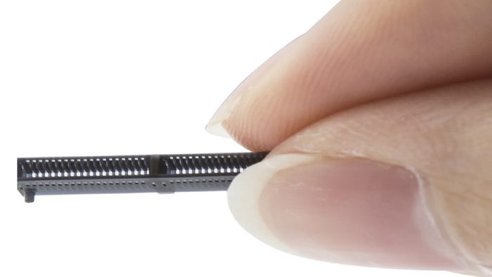
3D PrintingIndustry Voices: Is Micro-3D Printing the Future for Tiny Parts?Industry Voices: Is Micro-3D Printing the Future for Tiny Parts?
Additive manufacturing is becoming an efficient and cost-effective alternative to traditional micro-manufacturing methods such as molding.


Editors' Choice

.jpg?width=300&auto=webp&quality=80&disable=upscale)


Jun 4 - Jun 6, 2024
Jun 4 - Jun 6, 2024
Innovation in automation starts here. Discover and collaborate on automation solutions that are revolutionizing the entire production lifecycle — from design to production to market — and sharpen your competitive edge. ATX South is part of IME South, a six-in-one expo offering the latest insights & solutions spanning medtech, packaging, automation, plastics, design, & processing.
Register NowSign up for the Design News Daily newsletter.