Apptronik's Apollo robot totes a parts bin.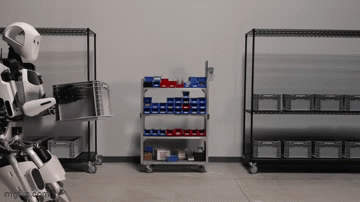
Automotive EngineeringMercedes Puts Apollo Robot to WorkMercedes Puts Apollo Robot to Work
Will Apptronik’s Apollo humanoid robot have to join the union?

.svg?width=700&auto=webp&quality=80&disable=upscale)


![BMW_IMG_Tank_400x219_0[1].jpg](https://eu-images.contentstack.com/v3/assets/blt0bbd1b20253587c0/blt7c572c44d4f2992a/65141676e94daff5a865dd1e/BMW_IMG_Tank_400x219_01.jpg?width=300&auto=webp&quality=80&disable=upscale "BMW_IMG_Tank_400x219_0[1].jpg")
![PTI-202006-AdobeStock_320996786[1].jpg](https://eu-images.contentstack.com/v3/assets/blt0bbd1b20253587c0/blt3cbef4e0e7dbd79a/65141675d3423181c28717fe/PTI-202006-AdobeStock_3209967861.jpg?width=300&auto=webp&quality=80&disable=upscale "PTI-202006-AdobeStock_320996786[1].jpg")

![2020-06-10-EXXO_6747_Primary-packaging_pillow-pouch-PT[1].jpg](https://eu-images.contentstack.com/v3/assets/blt0bbd1b20253587c0/bltc468009ddc4086a2/65141692092b4374895b466f/2020-06-10-EXXO_6747_Primary-packaging_pillow-pouch-PT1.jpg?width=300&auto=webp&quality=80&disable=upscale "2020-06-10-EXXO_6747_Primary-packaging_pillow-pouch-PT[1].jpg")


.svg?width=300&auto=webp&quality=80&disable=upscale "Fuel cell for wearables runs on sweat")
Editors' Choice


Jun 4 - Jun 6, 2024
Jun 4 - Jun 6, 2024
Innovation in automation starts here. Discover and collaborate on automation solutions that are revolutionizing the entire production lifecycle — from design to production to market — and sharpen your competitive edge. ATX South is part of IME South, a six-in-one expo offering the latest insights & solutions spanning medtech, packaging, automation, plastics, design, & processing.
Register NowSign up for the Design News Daily newsletter.