New material is the most effective ever at turning heat into energy
Researchers in Austria developed the material, which can be used to help sensors and other small devices run on autonomous power.
December 10, 2019

|
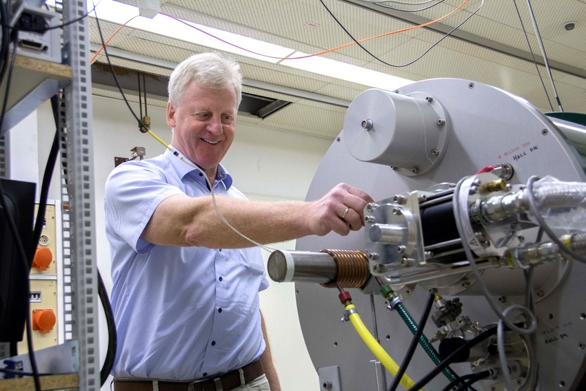
Professor Ernst Bauer in his lab at Vienna University of Technology, where he led the development of a new material with unprecedented effectiveness for converting heat to electricity. (Source: Vienna University of Technology) |
Researchers in Austria have developed material that they say is the most effective to date for converting heat into electrical energy. This unprecedented ability means the material could be used to provide an autonomous and renewable source of energy for a range of technologies, such as sensors or even small computer processors, by allowing them to generate their own power from temperature differences.
A material's ZT value measures the amount of electrical energy that can be generated at a given temperature difference; the higher the value, the better the thermoelectric properties. This new material—created by researchers at Vienna University of Technology – is comprised of iron, vanadium, tungsten, and aluminum applied to a silicon crystal, and has a ZT value of five to six, the highest ever measured for thermoelectric materials. Modern thermoelectric materials are maxed out at values of about 2.5 to 2.8.
“The difference is a much better performance of this material, about two times larger than the best reported so far in literature,” Ernst Bauer, the team lead, and a professor in the Institute of Solid State Physics at the university, told Design News.
Composition informs behavior
Key to the high thermal conductivity of the material is a “combination of several physical properties and parameters, Bauer told Design News.
The atoms in the material are arranged in what’s called a face-centered cubic lattice, he said. The distance between two iron atoms in the material is always the same, while the same is true for the atoms that comprise the other elements found in the material. This structure on its own is irregular.
When a thin layer of the material is applied to silicon, however, there is a dramatic change in its structure. The atoms still form a cubic pattern, but in a way that the distribution of the different types of atoms becomes completely random.
"Two iron atoms may sit next to each other, the places next to them may be occupied by vanadium or aluminum, and there is no longer any rule that dictates where the next iron atom is to be found in the crystal," Bauer said.
This change in the arrangement of the atoms also changes the material’s electronic structure, which protects the electrical charge—the portions of which are called Weyl Fermions – as it moves through the material from scattering processes, Bauer said. This results in a very low electrical resistance.
The Vienna University of Technology researchers published a paper on their work in the journal Nature.
While a thin layer of the material itself can’t generate enough energy to power even small devices, “it has the advantage of being extremely compact and adaptable," Bauer said. He and his team aim to use the material as a component of small-scale energy generators to provide power for sensors and other small electronic devices.
Bauer and his colleagues also will continue their work by seeking new
materials with similar properties and taking a deeper look into the one they developed “to understand on a microscopic basis all relevant phenomena occurring in this material,” he told Design News.
RELATED ARTICLES:
Elizabeth Montalbano is a freelance writer who has written about technology and culture for more than 20 years. She has lived and worked as a professional journalist in Phoenix, San Francisco and New York City. In her free time she enjoys surfing, traveling, music, yoga and cooking. She currently resides in a village on the southwest coast of Portugal.
About the Author(s)
You May Also Like


