Test Solutions for ‘Giga-Gate’ Designs
A new breed of test products is needed to handle of the challenge of chips that contain hundreds of millions, or even billions, of logic gates.
April 21, 2016
With logic gate counts on microprocessors soaring, chipmakers now face a vexing problem -- how to test a billion-gate chip in a reasonable amount of time.
The challenge of testing the so-called “giga-gate” devices has begun to affect more test engineers. New Oracle SPARC architectures, as well as product families from Apple and Intel, have created an unprecedented challenge. “There are definite complexities that arise when you get to hundreds of millions of gates,” said Stephen Pateras, product marketing manager for Mentor Graphics’ Silicon Test Division. “You start getting to the point where, instead of it taking hours or days to generate a test pattern, you’re into weeks or even months.”

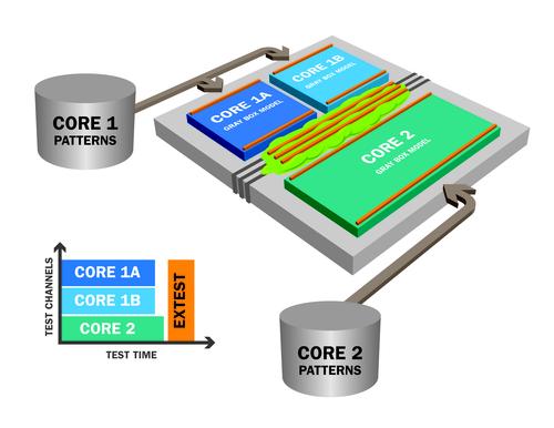
Mentor Graphics’ hierarchical approach reduces the pattern generation task into smaller, more manageable pieces. Compressed patterns are first generated for each core design in isolation. These patterns are then re-targeted to the chip level and merged to minimize test time. Compressed patterns are then generated for top-level interconnect and glue logic.
(Source: Mentor Graphics)
That, however, isn’t the only challenge. On some devices, chipmakers are adding functionality -- analog parts, RF transceivers, amplifiers, and sensors. And that, too, creates a test dilemma.
“The billion-gate discussion is not just about testing the same stuff faster,” said Luke Schreier, director of automated product marketing at National Instruments. “It’s about analog and RF capabilities baked into the silicon. It’s about complexity.”
The New Mathematics of Test
To fully appreciate the depth of the challenge, it’s best to first look back a decade or so. Back then, engineers would take a few hours to generate a test pattern on a workstation. Then they’d apply that pattern to a device-under-test for a period of time that could be measured in seconds.
Moore’s Law, however, gradually altered the mathematics of that process. As gate-counts graduated from the millions to tens of millions to hundreds of millions, everything changed. Pattern generation took longer. CPU requirements were greater. More patterns needed to be generated, meaning that the test process itself also took a few seconds longer. That, in turn, affected cost. Since device test can cost hundreds of dollars per minute, a change of even a few seconds mattered to the bottom line.
And the finger of blame pointed straight back to Moore’s Law. “When you had a million gates, it would take an hour to generate a pattern,” said Pateras. “But if you had a hundred million gates, it wasn’t just 100 times longer. It was non-linear. It took weeks or months. So the whole process eventually stopped scaling at some point. We had to re-examine what we were doing.”

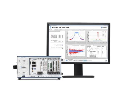
National Instruments says that by combining a vector signal transceiver, source measurement unit, and data acquisition module, 80% of all IoT applications can be successfully tested.
(Source: National Instruments)
Indeed, reassessment was necessary. That reassessment has led to the adoption of a hierarchical software approach. The hierarchical approach is essentially a “divide and conquer” methodology -- breaking up the problem into more manageable pieces using software products designed for that purpose. One such product, Mentor Graphics’ Tessent TestKompress, uses an on-chip compression technique to create smaller pattern sets that take less time to test.
“Instead of having to generate patterns for the whole design at once, you break up the problem,” Pateras explained. “Later, you can merge those patterns together very efficiently and very quickly to come up with a complete pattern set for the whole design.”
The result, Pateras said, is that CPU requirements drop and the number of needed patterns is halved. Moreover, reductions in runtime can fall by a factor of 5X to 10X.
Mentor said that its hierarchical technique is being adopted by a growing number of chipmakers. Mellanox Technologies, for example, cut the cost of generating its test patterns and reduced the processing time of its own ICs by employing the hierarchical approach. Equally important, the technique enabled design-for-test to be moved up earlier in the design cycle, which served as a scheduling advantage for engineers.
Pateras said that hierarchical technique still isn’t necessary in all cases, but as chip designs continue to evolve, it will become more pervasive. “People who have small designs probably don’t need the hierarchical approach now,” he said. “But once they get to 100 million gates, they’ll have almost have no choice.”
About the Author(s)
You May Also Like


