Chiplet Interconnect Technology Heads Toward Commercialization
Recently funded startup Eliyan expects to bring its high-performance chiplet interconnect technology to market in 2023.

The growing interest in chiplet technology for high-performance computing architectures has prompted both development among startup companies in conjunction with increased in funding activity. One such company, Eliyan Corporation, recently closed a Series A $40 million funding round and is set to unleash a chiplet interconnect technology, called NuLink, that achieves high performance using standard organic substrates.
Eliyan was founded by CEO Ramin Farjadrad, the inventor of Bunch of Wires (BoW) scheme, which has been adopted by the Open Compute Project (OCP). NuLink technology is backward compatible with Universal Chiplet Interconnect Express (UCIe), a standard developed by Intel and donated to the UCIe Consortium. According to Farjadrad, the technology achieves similar bandwidth, power efficiency, and latency as die-to-die implementations using advanced packaging technologies, but without the other drawbacks of more specialized approaches.
Eliyan’s BoW approach was specifically developed to address the need for highly efficient die-to-die (D2D) PHYs to connect different functions in one package. The NuLink technology, which is a superset of BoW and UCIe, uses patented implementation techniques to provide major power-performance differentiation for D2D connectivity over any packaging substrate, reducing complexity and lowering overall development time and costs.
Farjadrad, in an interview with Design News, said the technology eliminates the need for advanced packaging solutions, most commonly silicon interposers that limit overall system-in-package size that ultimately limits performance. The use of interposers also limits wafer test coverage that ultimately impacts yield, increases total cost of ownership, and extends overall manufacturing cycle time.
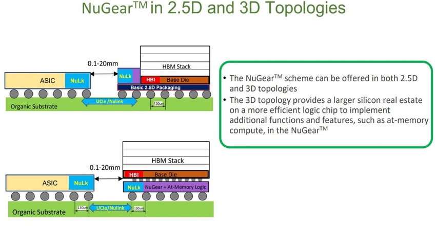
Instead of using interposers, NuLink uses a patented Gearbox scheme that acts as an adapter to connect any off-the-shelf chiplets with micro bumps over organic substrate with standard bump. This tec eliminates the need for a large complex silicon interposer. This optimized technology for 2.5/3D package implementations enables practical mix and match of chiplets with different die-to-die interfaces in in different processes (DRAM, SOI, etc.).
The technology has been under development by Farjadrad and his team since 2017. In 2018, Farjadrad proposed BoW as a superior chiplet interconnect architecture to OCP. The improved performance and features BoW offered over existing methods garnered strong support and eventual adoption as the chiplet interconnect scheme of OCP.
An earlier incarnation of the NuLink technology has been mass produced on a 14nm process, validating its commercial viability and performance advantages. The most recent version that was taped out at 5nm delivers minimum of 2000Gbps/mm of edge bandwidth on a standard organic package.
Eliyan expects its first silicon in the first quarter of 2023.
The ramp-up of Eliyan’s technology further hints of a bright future for chiplet technology, which is viewed as an important means of developing custom chips to help product developers scale the performance, power efficiency and size required by high performance computing applications.
Earlier this year, a group of leading tech companies recently formed an industry consortium to establish a die-to-die interconnect standard and promote an open chiplet ecosystem, called the UCIe consortium.
Spencer Chin is a Senior Editor for Design News covering the electronics beat. He has many years of experience covering developments in components, semiconductors, subsystems, power, and other facets of electronics from both a business/supply-chain and technology perspective. He can be reached at [email protected].
About the Author(s)
You May Also Like


