Tech Giants Form Consortium to Standardize On Chiplet Interfaces
Leading tech companies have formed an industry consortium to develop a standard interconnect scheme for chiplets, smaller die interconnected in a single package to provide multiple functions.

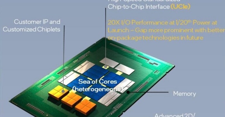
The increasing complexity of electronic systems is prompting more design engineers to look at chiplets, ICs that contain specific functions on separate die that are then interconnected and packaged together. One obstacle to greater acceptance has been developing a standard method to interconnect these dies, to improve design flexibility and sourcing.
In response, a group of leading tech companies─Advanced Semiconductor Engineering, Inc., AMD, Arm, Google Cloud, Intel , Meta, Microsoft, Qualcomm, Samsung, and Taiwan Semiconductor Manufacturing Company─recently formed an industry consortium to establish a die-to-die interconnect standard and promote an open chiplet ecosystem, called the UCIe consortium. The founding companies have ratified the UCIe 1.0 specification, an open industry standard developed to establish a package-level interconnect.
The specification covers the die-to-die I/O physical layer, die-to-die protocols, and software stack which leverages the well-established PCI Express�® (PCIe®) and Compute Express Link™ (CXL™) industry standards. The specification will be available to UCIe members and available to download on the UCIe website.
Combining Multiple Functions
The concept of chiplets has been around for over a decade, but the idea may have originated even further back in the 1960’s, when scientist Gordon Moore suggested in a technical paper, “It may prove to be more economical to build large systems out of smaller functions, which are separately packaged and interconnected.”
In a technical paper on the UCIe standard, author Dr. Debendra Das Sharma, Intel Senior Fellow and Chief Architect, I/O Technologies and Standards Promoter Member of UCIe, noted parts such as multi-core CPUs with core counts in the thousand could benefit from being configured as smaller die connected in a package, to improve yield optimization and promote die reuse.
Chiplets give engineers more flexibility in product design and can yield a time-to-market advantage. Functions can be implemented in different process nodes in a mix-and-match configuration depending on design goals. Engineers can, for example, implement the processor in a more advanced process node while memory, logic, and analog are implemented in less critical nodes.
Some companies are already incorporating chiplet technology in their products. For instance, Intel’s Intel® Stratix® 10 GX, SX, TX, and MX FPGA and SoC FPGA families and Intel® Agilex™ FPGA devices use chiplet technology to pair FPGA logic die with I/O tiles. AMD Ryzen™ Threadripper™ 3970X and 3960X high-end desktop processors uses a chiplet design with central I/O die supported by the company’s Infinity Fabric™ technology.
Both companies use different interconnect approaches in their Chiplet package designs. The UCIe protocol will standardize on a single approach that will make it easier for companies to source each other’s silicon in their products, potentially speeding time-to-market and cutting costs.
Layered Protocol
Because UCIe is an open standard with a plug-and-play model, the standard’s proponents believe it will be easily and widely adopted. UCIe will be a layered protocol. The physical layer is responsible for the electrical signaling, clocking, link training, sideband, etc. The Die-to-Die adapter manages the link state management and negotiates parameters for the chiplets. The protocol also provides cyclic redundancy check (CRC) and link level retry mechanism.
The standard defines two types of packaging: a standard 2D package for cost-effective performance, and an advanced package for power-efficient performance. The standard will support two broad usage models. The first is package-level integration to deliver power-efficient and cost-effective performance. The second usage model is to provide off-package connectivity using different media (optical, electrical cable, mmWave) using UCIe Property of Universal Chiplet Interconnect Express (UCIe) Retimers to transport the underlying protocols, to achieve power and cost goals.
According to UCIe, die with the standard package design is expected to interoperate with any other design on the standard package. In a similar vein, a die with the advanced package design will interoperate with any other die designed for the advanced package, even within the wide range of bump pitch from 25 u to 55 u.
UCIe member companies will later this year begin work on the next generation of UCIe technology, including defining the chiplet form factor, management, enhanced security, and other essential protocols.
Spencer Chin is a Senior Editor for Design News covering the electronics beat. He has many years of experience covering developments in components, semiconductors, subsystems, power, and other facets of electronics from both a business/supply-chain and technology perspective. He can be reached at [email protected].
About the Author(s)
You May Also Like


.jpg?width=300&auto=webp&quality=80&disable=upscale)


