How to Build a Better Chiplet Packaging to Extend Moore’s Law
Packaging approaches like chiplet tech can extend Moore’s Law. But what does that mean for chip design product developers and fabs?
September 13, 2021

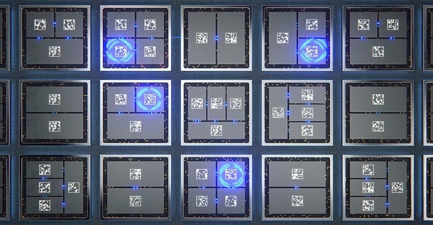
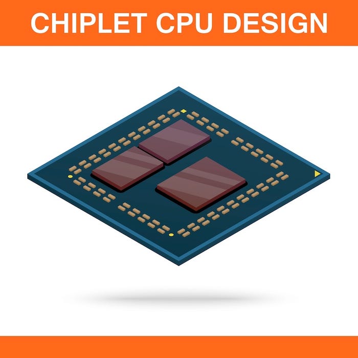
Moore’s Law may not be dead, but it certainly has been challenged significantly beyond the 28nm process node. Fortunately, there are ways to extend Moore's Law's cost, feature, and size benefits. One way is to use chiplets – or modular dies - that effectively bypass Moore’s Law by replacing single silicon die with multiple smaller dies that work together in a unified packaged solution.
This approach provides much more silicon to add transistors compared to a monolithic microchip. As a result, chiplets are expected to return to the two-year doubling cycle that has been the cornerstone economics of the semiconductor business since 1965.
The global market for processor microchips that utilize chiplets in their manufacturing process is set to expand to $5.8 billion in 2024, rising by a factor of nine from $645 million in 2018, according to Omdia. (Image Source: IEDM 2017, AMD Dr. Lisa Su keynote)

Many major chip manufacturers are incorporating chiplets into their designs. For example,
Intel recently revealed additions to its advanced packaging strategy and introduced two new 3D chip stacking technologies—Foveros Direct and Foveros Omi. Both packaging technologies will be ready for mass production by 2023. The former involves a base die on which chiplets can be stacked. Conversely, Omni will allow the base die to be a different size from the top die.
Chiplets are not without challenges, but they do provide many benefits. With a chiplet methodology, a vendor may choose from a menu of modular dies in a library. Chiplets can have different functions and process nodes that can be mix-and-matched and then assembled in an existing advanced package or a new architecture.
Drivers
What is driving the trend toward chiplets? According to Dr. Amin Shokrollahi, Founder and CEO of Kandou, there is a combination of five factors:
The rising cost of taping chips out. Mask sets themselves can be multiple millions of dollars.
The tendency toward ever-larger chips. Some have reached the reticle limits, and others have just suffered from yield loss.
The availability of multiple technologies to bind chiplets together, including fine-geometry and traditional organic package substrates.
The need to have each function in a process node and foundry that is specific to that function. Chiplets allow mixing and matching different geometries and different foundries.
The need for flexibility in product offerings to meet various market requirements. Chiplets enable multiple products to be made from the same few chiplets.
Designing for Chiplets
How can chip designers take advantage of chiplet packaging for their products? While the significant semiconductor EDA tool companies provide proprietary software, chiplet tools are not yet accessible to most of the market. Further, standards are still being developed for this emerging technology. But there are key considerations that will help today’s designers.
It’s important to realize that using fine geometry interconnect between chiplets incurs some yield loss, manufacturing complexity, and overall headaches, explains Shokrollahi.
“There are ways to effectively integrate chiplets that avoid the use of fine-geometry interconnect altogether,” said Shokrollahi. “Using SerDes to connect chiplets mounted on traditional organic package substrates avoids these problems. Low-power, ultra-short reach USR/XSR SerDes is the preferred solution for the high-speed interconnections between the chiplets.”
There is an art to carefully sub-dividing a large chip into tiles. Done well, benefits can be large. One common mistake is having an I/O chiplet that only has a SerDes that results in this I/O chiplet being too small, wasting the opportunity to shrink the larger main processing tiles. A better method, says Shokrollahi is to put as much of the I/O subsystem as possible on the I/O chiplet. This can include the TCP offload, packet segmentation, credit management, forward error correction, and framing blocks, as well as the SerDes. This solution requires a fatter pipe going to the I/O chiplet than is needed for just the SerDes.
Processing chiplets can often be replicated in tile form. These tiles enable different products with differing counts of chiplet tiles. Only two types of chiplets are needed in this tile solution, one tile chiplet, and one I/O chiplet. A router fabric or torus network is often devised to manage connections between tiles that are not attached to each other.
Two projects from the Optical Internetworking Forum (OIF) will produce Interoperability Agreements (IAs) for the SerDes that connect chiplets, note Shokrollahi. The first is CEI-112G-MCM (Multi-Chip Module) project, and the second is the CEI-112-XSR project. The MCM project uses CNRZ-5 modulation; the XSR project uses PAM-4 modulation. Both ongoing projects have different properties and are optimized in different ways. SerDes based on the MCM IA may be lower power and are useful in fat-pipe applications. SerDes based on the XSR IA are useful in thin-pipe applications and are more compatible with existing systems.
Using SerDes with either of these two IAs to connect chiplets within an MCM simplifies development because they avoid fine-geometry interconnects such as Chip-on-Wafer-on-Substrate (CoWoS) or INFO, cites Shokrollahi. SerDes implementations have slightly more latency than those that use wires over a fine-pitch interposer. However, the slow clock rate of the low-speed interconnects means that those solutions are likely to have a latency of at least two slow clocks. SerDes solutions also have error rates that must be addressed. XSR PAM-4 SerDes implementations aim to improve a raw error rate of 1E-9 through traditional Forward Error Correction (FEC) blocks. MCM CNRZ-5 SerDes implementations aim for a raw error rate of 1E-15 improved with minimal, low-latency FEC.

John Blyler is a Design News senior editor, covering the electronics and advanced manufacturing spaces. With a BS in Engineering Physics and an MS in Electrical Engineering, he has years of hardware-software-network systems experience as an editor and engineer within the advanced manufacturing, IoT and semiconductor industries. John has co-authored books related to system engineering and electronics for IEEE, Wiley, and Elsevier.
About the Author(s)
You May Also Like


.jpg?width=300&auto=webp&quality=80&disable=upscale)


