Cheeky Chiplets Meet Super NoCs
There’s a whole new semiconductor implementation technology headed our way.
August 22, 2023
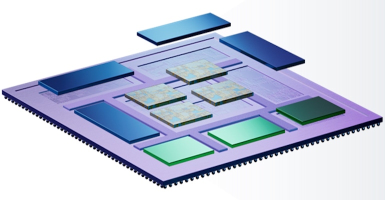
I’ve been seeing more and more activity on the chiplet front recently (multiple silicon dice on a common substrate). Several of the big players have been using proprietary in-house implementations for some time, but things seem to be moving such that—in the not-so-distant future—everyone will be able to join in the fun.
Before we leap headfirst into the fray with gusto and abandon (and aplomb, of course), it might be useful to define a few terms to ensure we are all tap-dancing to the same skirl of the bagpipes.
Let’s start at the beginning with integrated circuit (IC), which refers to a circuit formed from a collection of components (transistors, resistors, etc.) implemented on a small flat piece of semiconductor material. Although a variety of semiconductors may be used, silicon is the most common, so these devices are generically referred to as “silicon chips.”
The phrase monolithic integrated circuit is often used to reflect and emphasize the fact that everything is implemented on a single, solid, seamless piece of silicon, thereby distinguishing these circuits from their predecessors, which were created using collections of discrete (individually packaged) components.
ICs can be analog, digital, or mixed-signal (both analog and digital) in nature. I’m not going to make mention of radio frequency (RF) devices because just thinking about what it takes to design one makes my head hurt.
The terms ASIC, ASSP, and SoC are often a source of confusion for the unwary. As I wrote in my book Bebop to the Boolean Boogie: An Unconventional Guide to Electronics (which I often use for a reference myself): "Generally speaking, an Application-Specific Integrated Circuit (ASIC) is a component that is designed by and/or used by a single company in a specific system. By comparison, an Application-Specific Standard Product (ASSP) is a more general-purpose device that is created using ASIC tools and technologies, but that is intended for use by multiple system design houses. Meanwhile, a System-on-Chip (SoC) is an ASIC or ASSP that acts as an entire subsystem including one or more processors, memory, peripherals, custom logic, and so forth."
There are several things worth noting here. When they hear the terms ASIC and ASSP, many people’s knee-jerk reaction is to think of digital devices, but that’s because those people come from the digital domain. Analog designers may well consider their purely analog creations to be ASICs and ASSPs. Analog aficionados are also fond of saying that digital is a subset of analog, which explains why they don’t have many friends and tend to end up standing alone in the corner at parties. Having said this, even “purely digital” devices containing mindboggling quantities of digital functions will almost invariably include a handful of analog elements to monitor things like voltage and temperature, along with some larger analog functions like phase-locked loops (PLLs).
Circa the 1970s, it was common to have only small amounts of digital logic implemented in an IC (I’m thinking of 7400-series devices from Texas Instruments and 4000-series components from RCA). Printed circuit boards (PCBs) in those days might carry hundreds of these components. Over time, we moved to having fewer devices, each containing more digital functions.
Each semiconductor process has rules on the minimum size for structures that can be fabricated on the chip. Each new generation process is known as a technology node or process node, designated by the minimum feature size that can be achieved by that process (I’m simplifying things, but I’m sure you get the gist). Historically, these feature sizes (hence, process nodes) were specified in millionths of a meter (micrometers or µm). The first ASICs I designed circa 1980 were Toshiba devices implemented at the 5-µm node. These days, process nodes are specified in billionths of a meter (nanometers or nm).
Over the years, as geometries (the sizes of structures on chips) shrank, it became possible to squeeze more and more transistors into the same area. Also, advances in fabrication tools and technologies made it possible to create larger and larger dice (chips). How large? Well…
Pause to take a deep breath… In 1996, the Intel Pentium Deschutes, which was implemented at the 0.25-µm (250-nm) process node, had 7.5 million transistors, which was a staggering number at that time. In 2003, the IBM PowerPC 790, which was created at the 90-nm process node, comprised 58 million transistors. In 2007, the Intel Xeon 5400, which was fabricated at the 45-nm process node, contained 820 million transistors. In 2010, the Intel Westmere-EX, which was manufactured at the 32/28-nm process node, featured 2.6 billion transistors. In 2018, the Apple A12 Bionic, which was realized at the 7-nm process node, boasted 6.9 billion transistors. More recently, in 2022, the Apple A16 Bionic, which entered the fray at the 4-nm process node, flaunts 15+ billion transistors… and breathe out again (phew!).
On the one hand, this is all jolly exciting. I know of several relatively small startup companies that have created multi-billion transistor devices. On the other hand, we are reaching the bounds as to what can be achieved with today’s technologies. For example, the theoretical limit for a photomask used with the extreme ultraviolet (EUV) process is ~850 mm2 (around 29 mm x 29 mm square). In practice, as we pass ~600 mm2 (say 25 mm x 25 mm), the yield—that is, number of chips that work vs. the number that don’t—starts to fall off dramatically (sad face).
Splitting the functionality into multiple, individually packaged devices isn’t an option (well, it’s not a good option) because of the power consumption and delays associated with the chip-to-chip (C2C) interconnect. The solution is to take multiple dice—which, in this context, are commonly known as chiplets—and mount them on a common substrate. This substrate can be organic,* like a small, high-density PCB, or semiconductor, and the result is known as a multi-die system (*the term organic is used in this context because the molecules forming the plastics and resins in the substrate have a “backbone” formed from carbon atoms, and carbon is the key element for organic life as we know it).

I was just chatting with the guys and gals at Synopsys about all of this because they have been beavering away on the tools and technologies required to design and verify multi-die systems of this ilk, all the way from silicon IP to chiplet IP to multi-die architectural exploration and multi-die packaging.
The chaps and chapesses at Synopsys say that, thus far, they’ve identified four main chiplet use cases. The first scenario is to simply mount multiple copies of the same die onto the substrate, like an array of CPUs, GPUs, or NPUs, for example. The second scenario is to take a design that you would really like to implement on a single monolithic die, but that die would be too large and the yield would be too low, so you are obliged to split it into two or more chiplets.
The third scenario is based on the fact that, while you may wish to implement the main digital device functionality at the latest-and-greatest process node you can afford, this node may not convey any benefits for some input/output functions like high-speed transceivers. Furthermore, considering that functions like transceivers involve a complex mix of sophisticated analog and digital functionality, once you have one working in one process node, you may wish to stick with this existing, proven, risk-free solution. A great example of this scenario is provided by Intel Agilex 7 FPGAs and SoC FPGAs (where an SoC FPGA includes a hard processor subsystem, or HPS for short).
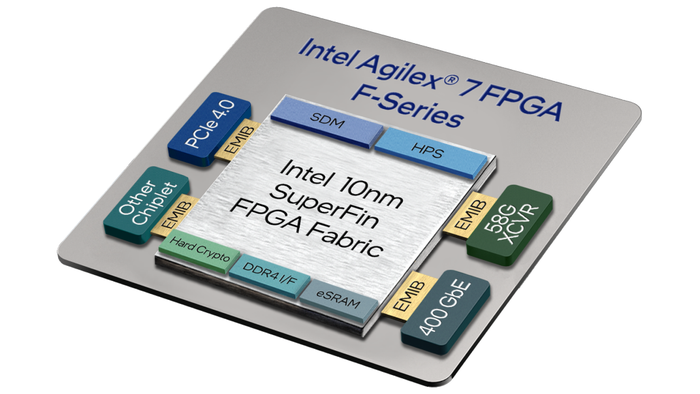
In addition to the main die, Intel Agilex 7 devices contain two to six transceiver (XCVR) chiplets, which they call tiles. These XCVR tiles, which can support 400 Gbps Ethernet, PCIe, and Compute Express Link (CXL) interfaces, are connected to the main FPGA die using Intel embedded multi-die interconnect bridge (EMIB) technology.
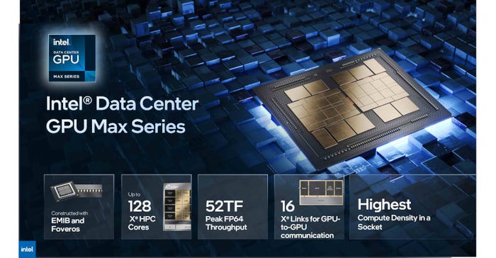
The final scenario involves disaggregating the functionality of the device into multiple heterogeneous dice, each implemented at the optimal node (in terms of cost, power, performance, etc.) for its function. For example, an RF die might be implemented using a 28-nm process node, a die containing high-speed analog-to-digital converters (ADCs) could be implemented in a 16-nm process node, and any “secret squirrel” digital logic may be realized using a 5-nm process node. The most mindboggling example I’ve seen of this sort of thing is the Intel Data Center GPU Max Series of devices (these used to be known as Ponte Vecchio GPUs). I mean to say—47 tiles and 100+ billion transistors—what’s not to love? (I’m only glad I wasn’t put in charge of counting all the transistors.)
So far, so good. But there’s one part of this puzzle we have not yet considered, which is how do the chiplets “talk” to each other using die-to-die (D2D) interconnect. To be honest, I hadn’t even thought about this until the folks at Synposys mentioned that they were partnering with Network-on-Chip (NoC) companies because, as they told me, “We want NoCs in multiple chiplets to behave as a single super-NoC offering the highest possible bandwidths with the lowest possible latency.”
The mere mention of a “Super NoC” set all sorts of ideas bouncing around my poor old noggin. On the off chance NoCs are new to you, let me give you a very brief overview. The sort of ICs we are talking about here are formed from functional blocks known as intellectual property (IP) blocks. In ancient times (prior to the year 2000), an IC might contain a relatively small number of relatively small IPs, all of which communicated with each other by means of a bus. As the number of IPs and the size of those IPs grew, developers started to employ crossbar switches. But the numbers and sizes of IPs continued to grow, causing crossbar switches to run into congestion problems and run out of steam.
The solution was to move to a NoC. Let’s remind ourselves that each IP will have its own interface characteristics (data width, clock frequency, etc.). Also, each IP will employ one of the many standard protocols that have been adopted by the SoC industry (OCP, APB, AHB, AXI, STBus, DTL, etc.). The solution is for each IP to be connected to a function called a socket (again, I’m simplifying things a bit). In the case of an IP that wishes to transmit data, its associated socket will packetize and serialize the data into a normalized form suitable for transport over the network. Like a regular network, multiple packets passing between multiple IPs can be in flight at the same time. When a packet arrives at its destination, the socket attached to the destination IP will convert the incoming packet back into whatever form is employed by that IP.
NoCs can be implemented in all sorts of topologies, some simple examples of which I’ve shown below. In some cases, a chip may employ multiple NoCs, such as a 1D tree covering one part of the IC and a 2D mesh addressing the requirements of another portion of the device, for example.
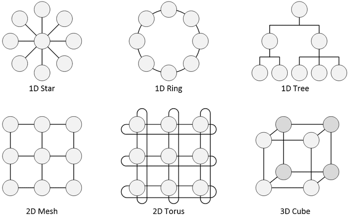
In fact, many IP blocks are now so large that they employ their own NoCs inside—maybe we should call these Networks-in-IPs (NiPs) but remember this is just something I made up on the fly—and then each of these NiPs is connected to the main chip’s NoC. So, it makes sense that if we want to implement the D2D interconnect between the chiplets forming a multi-die system, then a Super NoC would be one way to go.
Wanting to learn more, I called up my friend Frank Schirrmeister, who is Vice President Solutions and Business Development at Arteris IP. If anyone knows what’s going on in the world of NoCs, it’s the folks at Arteris. For example, there’s an Arteris NoC in 70% of the SoCs used to power Advanced Driver Assistance Systems (ADAS) in automobiles around the world.
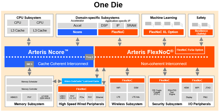
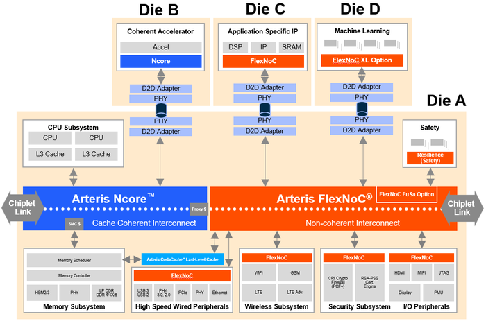
Frank pointed out that when you wish to have your NoC cross the chiplet boundary as part of a D2D implementation, you are going to have to consider whether you need your chiplets to be cache coherent or not (Arteris offers FlexNoC for applications requiring non-coherent interconnect and Ncore for applications requiring coherent interconnect), the protocol layer (PCIe, CHI, AXI, CXL, CCIX, proprietary…), the link layer (packetization via AMBA, CXS, CPI, proprietary…), and the physical layer (PCIe, BoW, UCIe, XSR…).
The way I’ve typically seen Arteris NoC interconnect IP technology presented graphically is as shown below.
However, since I was now expressing my interest in the concepts of Super NoCs used in the context of D2D chiplet interconnect in multi-die systems, Frank was kind enough to share a corresponding graphical depiction as shown below.
There’s so much more to discuss here. For example, we could spend days (possibly weeks) unpicking the intricacies of the various acronyms I’ve been throwing around (PCIe, CHI, AXI, CXL, CCIX, AMBA, CXS, CPI, BoW, UCIe, XSR…).
Take the folks at Eliyan, for example, who say their NuLink D2D interconnect solution delivers a UCIe-compliant interconnect at twice the bandwidth and half the power (I’m hoping to have a chat with them about this in the not-so-distant future).
Also, I was recently chatting with Mateus Grellert, who is an Assistant Professor at Universidade Federal do Rio Grande do Sul (UFRGS). As Mateus told me, “Our research group at UFRGS is currently working with our industry partners on projects related to the development of chiplet-based systems, including design methodologies, communication interfaces, and tools that can accelerate time to market.”
Mateus went on to say that the communication strategies and protocols they were looking at included NoCs and NoPs. When I asked about the NoP nomenclature with which I was unfamiliar, Mateus replied: “NoP means Network-on-Interposer. It's the SiP version of a NoC. I'm not sure if it's a coined term yet, but I stumbled upon it in a paper I was reading on chiplet-based Scalable In-Memory Acceleration (SIAM).”
I tell you—I learn something new every day. I’m going to spend some time talking to more people so I can learn the ins and outs of all this. In the meantime, as always, I welcome your captivating comments, insightful questions, and sagacious suggestions.
About the Author(s)
You May Also Like


