Reincarnated Return of the HRRG 4-Bit Computer (Part 2)
The HRRG’s design has evolved over the years, cumulating in a new collection of CPU registers (both physical and virtual).
May 7, 2022

In my previous blog, I reintroduced the concept of the Heath Robinson Rube Goldberg (HRRG) 4-bit computer, which has been on my “To Do” list for more years than I care to remember.
As we discussed, after pondering this project on my own for a couple of years, I was introduced to Joe Farr who lives in the UK and who I now count amongst my closest friends. As the years have gone by, Joe and I have oscillated between working on the HRRG furiously to the exclusion of all else, to pushing it onto the backburner when something else grabbed our attention.
We were in this latter state in early 2021 when I received an email from an engineer named Nils van den Heuvel, who hails from the Netherlands. Nils said that he had run across some of my HRRG writings and that he was interested in creating an FPGA-based implementation of the HRRG, so Joe, Nils, and I started to have weekly meetings to bounce ideas around.
When I started to write this column, I asked Nils to pen a few words to introduce himself, and he responded as follows:
I am an electronics engineer. I graduated in 1993 from the University of Twente (Netherlands, Europe). My first job was setting up a condition monitoring system for a wood grinding installation in Nijmegen. Then I started creating electronics designs in Bunschoten by developing electronics for drilling, lathing, and milling machines. As suggested by one of my colleagues, I used FPGA technology to realize a fully integrated and digitized servo control running at 1 MHz. Later, I moved to Middelburg to design the main board and sensor electronics for analytical instruments, after which I worked on high voltage accelerators in Amersfoort. For an implanter, I designed a 500 kHz bandwidth ultra-precise beam profile generator with FPGA logic control. Currently, I am living in Eindhoven, focusing on developing electronics for the world’s best lithography machines.
As I mentioned in my previous blog, there’s nothing like trying to build something to reveal any holes in your design. Once Nils had embarked on his implementation, he started to run into issues with our original specification, which led to a bunch of changes. I’m not going to discuss every nitty-gritty detail here, but I will touch upon some of the more interesting changes for those who have been following this since the HRRG was naught but a twinkle in my eye.
As an aside, in the same way the term “byte” is used to indicate an 8-bit quantity, the term “nybble” reflects a 4-bit value, hence the joke “two nybbles make a byte” (I didn’t say it was a good joke).
Just to set the scene, we’ve decided to use the % character to indicate binary values and the $ character to indicate hexadecimal values. The HRRG has a 4-bit data bus and a 12-bit address bus. Each 4-bit nybble of data can adopt one of 16 values ranging from 0 to 15 in decimal, %0000 to %1111 in binary, or $0 to $F in hexadecimal. Similarly, our 12-bit address bus spans the range 0 to 4,095 in decimal or $000 to $FFF in hexadecimal.
Let’s start with the central processing unit (CPU) and its internal registers. When you come to think about it, if we exclude any weird and wacky architectures, the minimum set of registers with which a CPU can get by would be a program counter (PC), which keeps track of where we are in the program; a register used to accumulate (hold) the results of any operations; and a register used to store the status flags associated with any operations (individual bits of this register can be implicitly or explicitly read and/or written by the machine code instructions executing on the processor).
Many of the early 8-bit microprocessors had a single 8-bit accumulator (ACC), which was used to store the results from intermediate operations, like adding two 8-bit values together. Meanwhile, the status register (SR) was used to keep track of the state of the machine by means of a set of 1-bit status flags. In the case of an 8-bit addition, for example, the Z (zero) flag would be used to indicate if the result from the addition was zero, the N (negative) flag would be used to indicate if the result from the addition was negative (3 + -5 = -2, for example), the C (carry) flag would be used to indicate if there was a carry-out bit from the addition, and the O (overflow) flag would be used to indicate if an arithmetic overflow had occurred, which would indicate that the signed two's complement result from the operation would not fit in the ACC (we will discuss this in more detail in a future column).
The early days of 8-bit microprocessors were quite exciting, because each new machine featured its own architectural innovations. Some CPUs sported two accumulators (ACCA and ACCB), for example, while others augmented their single ACC with a handful of general-purpose registers, and some discarded the ACC and just went with general-purpose registers.
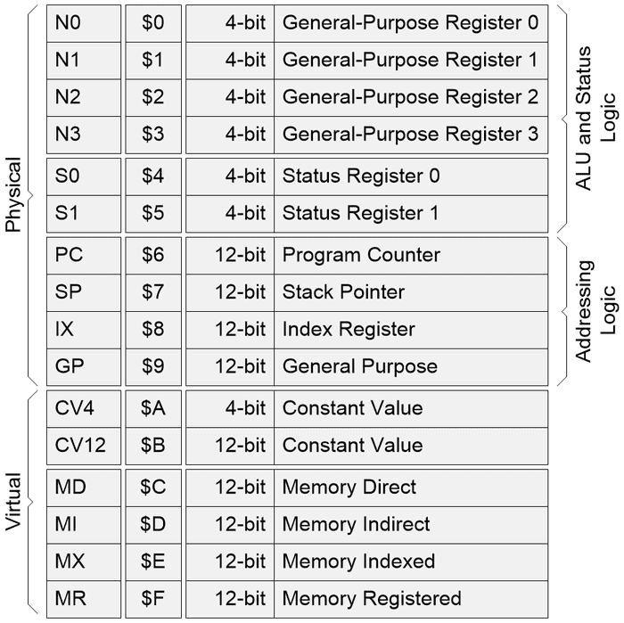
In the case of the HRRG with its 4-bit word size, we want to be able to uniquely identify each register using a single nybble, which obviously limits us to only 16 registers. The names, sizes, and functions of these registers have evolved over time. The latest and greatest set that we’ve finally agreed on and locked in stone (touch wood) is illustrated below.

At the heart of a CPU we find its algorithmic logic unit (ALU), which is where all of the number-crunching and decision-making is performed. In the case of our HRRG 4-bit computer, we’ve done quite a few things that we haven’t seen anywhere before, so it’s worth taking a few moments to walk through these architectural features. First, we’ve divided our registers into two main types: physical and virtual. In the case of the physical registers, there are two further sub-divisions into the ALU and status logic on one side, and the addressing logic on the other.
As we see, we have four 4-bit general-purpose registers, N0 to N3. Since we have more status bits than we’ve discussed thus far, we also have two status registers, S0 and S1. In the case of the addressing logic, we have four 12-bit registers—in addition to the PC, we also have a stack pointer (SP), an index register (IX), and a general-purpose register (GP). In our earlier incarnations, we also had a 12-bit interrupt vector (IV) register as part of the addressing logic. The idea was that we could load this register with the address of an interrupt service routine (ISR), and that the PC would jump to this address if an interrupt occurred. More recently, we decided to simply store the 12-bit address for the ISR in the three most significant nybbles of the memory at addresses $FFD, $FFE, and $FFF.
With respect to the virtual registers, these are used to implement constant values and different addressing modes. We started off with a single CV (constant value) register, leaving it up to the CPU to decide whether it was looking for a 4-bit or a 12-bit source value depending on whether the target was a 4-bit or 12-bit register, for example. But this approach led to Nils running into some subtle issues. In turn, this led to us replacing the CV register with a 4-bit/1-nybble CV4 register and a 12-bit/3-nybble CV12 register (we also refer to 3-nybble values as trybbles, not least because we are all fans of "The Trouble with Tribbles" episode in Star Trek: The Original Series).
We can think of the virtual registers as being the mechanism used to implement various addressing modes. For example, the CV4 and CV12 virtual registers implement the immediate addressing mode. The remaining virtual registers, MD, MI, MX, and MR, implement the direct (or absolute), indirect, indexed, and registered addressing modes, respectively (we will discuss what all this means in future columns).
Lest you think we are making all of this up (“What are you waffling on about with your virtual registers,” I hear you cry), may I be so bold as to remind you that the 8-bit Intel 8008 microprocessor, which was introduced in 1972, also employed a rudimentary form of virtual register. I invite you to visit Nils Eilers’ Intel 8008 Support Page where he notes (I’ve made some tiny edits): “The 8008 microprocessor contains an accumulator A plus six scratch registers B, C, D, E, H, and L, each 8-bits wide. The combination of H and L acts as a pointer to memory, providing a virtual register M. This is the only way to access the memory on the 8008.”
So, what do you think so far? Are you as excited as am I to see my next blog in which we will dive into the HRRG 4-bit computer’s instruction set? Just to give you something to think about, we are using a single nybble to specify the instruction, which means we are limited to only 16 instructions. If this was your computer, which set of 16 instructions would you implement? Until next time, as always, I welcome your comments, questions, and suggestions.
About the Author(s)
You May Also Like


