How to Design PCBs Faster (Much, Much Faster)
From architectural block-diagram to schematic in 60 seconds flat!
February 23, 2024
At a Glance
- Silicon is a mix of three stable isotopes (28Si, 29Si, & 30Si). It’s possible using only 28Si will result in faster chips
- A new PCB design tool can convert an architectural block diagram into a corresponding schematic & BoM in 60 seconds
I’m sure that, following Part 1 and Part 2 of my How to Pick and Program a PIC mega-mini-series, you were expecting to see Part 3… and you will… but not today because we have other poisson à frire (fish to fry).
My head is buzzing with myriad new tidbits of trivia and nuggets of knowledge. As a starting point, supposing I were to tell you that I know a man who knows a way to make silicon chips run much faster while consuming less power?
Obviously, we are doing this sort of thing all the time by migrating to new process nodes (also known as technology nodes or just nodes), where these terms refer to semiconductor manufacturing processes. When I wore a younger man’s clothes, the way we thought about this was that the number associated with a process node represented the size of the smallest physical structure that could be created in or on the surface of the chip. The sort of features we were talking about might be the width of a track or the length of the channel between the source and drain regions of a field-effect transistor (FET). The first ASICs I designed were implemented at the 5-µm (five micron) note, where 1 µm is one millionth of a meter.
Unfortunately, this way of thinking about things was always a little fluffy around the edges, and it got even flakier when we moved below the 28-nm node, where 1 nm is one billionth of a meter. Today, companies working at the “bleeding edge” are creating devices at the 3-nm node, such as Apple’s A17 Pro processor, which flaunts over 19 billion transistors on a single silicon die!
This sort of thing is OK for behemoth semiconductor foundries (a.k.a. fabs) like TSMC, but what about lesser-known players, like SynchroLux, for example? These guys are small and “light on their feet,” as it were. They are ideal for tasks like early-stage prototyping and low-volume production projects. Unlike the bigger fabs, which can take months to even notice you exist, a fab like SyncroLux can be up-and-running on your project within a week of you signing the (very affordable) purchase order. Even better, SynchroLux also offers packaging services, thereby making it a true “one-stop-shop.” The reason I’m waffling on about the folks at SynchroLux here is that they predominantly work at the 180-nm process. Although this may sound large as compared to the 3-nm process, there is a huge market for devices manufactured using affordable, mature, and low-risk technologies like the 180-nm node.
Now suppose we could make silicon chips implemented at the 180-nm node run 10X or even 100X faster? I bet that would make those who don the undergarments or authority and stride the corridors of power sit up and take notice.
“But how might this be possible?” I hear you cry. Well, let’s start with the fact the silicon used to make integrated circuits requires an ultra-high purity of 99.999999999%. This is known as the “eleven nines.” That’s an amazing level of purity, right from the get-go. However, silicon has three stable isotopes: 28Si (92.23%), 29Si (4.67%), and 30Si (3.10%). This is where all sorts of wibbly-wobbly quantum effects come into play, but I’m informed that—if we could somehow remove the 29Si—then chips formed using only 28Si and 30Si will perform their magic orders of magnitude faster. This could be a game changer.
Of course, extracting the 29Si is a tad tricky. However, I was just chatting with the folks at a company called ASP Isotopes. These little scamps are in possession of a jolly interesting technology that makes removing the 29Si both feasible and affordable. I shall be reporting further in future columns.
“Ah,” you say, “but that’s just the silicon chips. Don’t you have anything to offer at the printed circuit board level?” Why yes, I do (at least insofar as the wires used to connect boards to the rest of the system). As was recently reported here on Design News, "Graphene Has Been Found to Boost the Conductivity of Copper." It seems that adding graphene to electrical-grade copper reduces a wire’s temperature coefficient of resistance without impacting its electrical conductivity. Many embedded systems are required to run in hot environments, heat increases the resistance of wires, and higher-resistance wires generate more heat (it’s like the circle of life, but not in a good way). We certainly do live in interesting times.
But none of the above is what I wanted to talk to you about.
The reason for my current excitement—and for this column—is that I was recently chatting with Tomide Adesanmi, who is the Co-Founder and CEO at Circuit Mind. Their tag line is, “From Architecture to Schematic in 60 Seconds.” I can hear you thinking, “pull the other one, it’s got bells on it” (or words to that effect), but I’ve seen it working, and it’s true!
The easiest way to describe how this works is to look at the screenshot of their Assistant to Circuit Engineers (ACE) interface below.
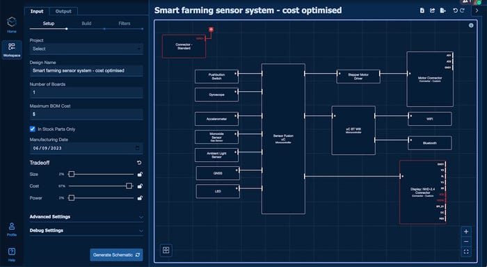
Capturing an architecture with ACE. CIRCUIT MIND
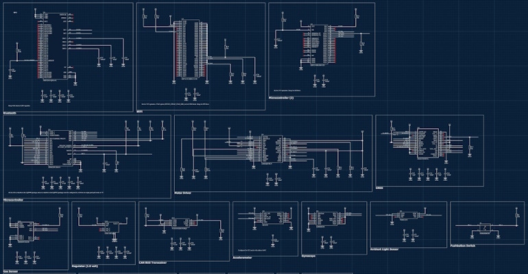
“Under the hood” is a huge library of digital twin components. Anything (useful) you can read in a data sheet is captured in a machine-readable and machine-understandable form. You start by creating your design architecture at a block level of abstraction. You use a drag-and-drop approach to select blocks from the library—where these blocks represent sensors, actuators, microcontrollers, etc.—and place them in your working area. As part of this, you also add simple connections indicating only what is connected to what. For each block, you can leave it “as-is” or you can add as many attributes as you wish. In the case of a microcontroller, for example, you can leave it up to ACE to select the best one for your particular project, or you can start specifying things like bus width, memory size, manufacturer, family, all the way to a specific part and package. You also use sliders to specify your desired tradeoffs between size, power consumption, and cost. When you are ready to rock-and-roll, you press the “Go” button and… within a minute or less… you are presented with a schematic as illustrated below.
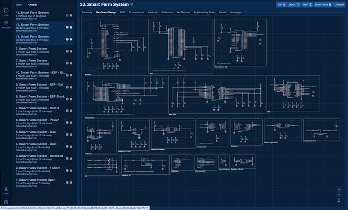
The resulting auto-generated schematic. CIRCUIT MIND
The generated schematic includes any required components like pull-up and pull-down resistors, decoupling capacitors, level-translators, etc.
Tomide tells me that this technology is aimed at professional engineers, not hobbyists. He also tells me that several “name brand” companies are already ACE to create real-world designs. I know a lot of professional engineers who will say something like, “I can design something much better than a computer program can.” I’m not arguing with that, but I would ask, “Can you do it in 60 seconds?”
An important related consideration is that, by tweaking your tradeoff parameters, you can quickly and efficiently explore the solution space by generating a suite of candidate designs that you can subject to more in-depth evaluation.
I, for one, think this is a very exciting development. What about you? If you are interested in learning more, the formal unveiling of this technology in the form of an online public demonstration is set to take place on Thursday 29 February 2024 at 11:00 am Central Time in the US and Canada. If you register now, the folks at Circuit Mind will be happy to email you a reminder closer to the day. Maybe I’ll see you there. :-)
About the Author(s)
You May Also Like


