Top-Side Cooling MOSFETs Boost Automotive System Density
Benefits include better power dissipation, lower temps.
July 26, 2023

Ramiro Gascon, Product Line Manager, On Semiconductor
Alongside full electrification, fully autonomous driving will be the next big paradigm in vehicle design and manufacturing. Even today, semi-autonomous driving, enabled by advanced driver assistance systems (ADAS), has already significantly increased the number of electronic control units (ECUs) managing a broad range of applications, including data fusion from external sensors and onboard cameras. The power consumption of these controllers is increasing in line with the volume and speed of data processing.
The new controllers require voltage regulators with power output capacities from low single-digit watts for an ECU managing parking assistance sensors up to 100+ W for an ECU processing multiple video streams. Heat generation is an inevitable side-effect of power dissipation, which limits how closely components can be placed on a PCB to prevent overheating. This is especially problematic for OEMs of electric vehicles where space and weight negatively impact range.
Effective thermal management is critical for high-power step-down conversions in automotive applications. Conventional bottom-side cooling (BSC) techniques have limitations, and new solutions are required as power densities continue to increase. But an innovation in component packaging, Top Side Cooling (TSC), can help address the problem of excess heat dissipation, enabling higher power density in smaller, lighter automobiles.
Bottom Side cooling
Recently, most surface-mounted devices (SMD) in high-power applications employed BSC (bottom-side cooling) to dissipate the heat from the silicon die. A metal pad on the bottom of the SMD package is connected through board vias to a heatsink underneath the PCB. However, there are some potential pitfalls to this approach:
The temperature rise inside the PCB itself could negatively impact the operation of other components mounted nearby on the PCB.
The PCB could suffer delamination if subject to elevated temperatures for an extended period, thus reducing the system lifespan.
Figure 1: SMD with bottom-side cooling: heat flows through vias and PCB.
Top Side Cooling
TSC offers a more direct thermal path for heat dissipation and enables better heat transfer from the power semiconductor device to an attached heat sink. Compared to BSC, it can provide up to 70% improvement in thermal performance, reducing system operating temperatures and improving efficiency, both critical for high-power step-down voltage conversion in automotive applications. In addition, TSC offer additional benefits for PCB design beyond excellent thermal performance.
Figure 2: SMD with top-side cooling: no need for thermal vias.
Improved Mechanical Stability
Attaching a heat sink directly to the top of a package significantly reduces the risk of mechanical stress or damage to the device or board, improving the reliability and extending the lifespan of components.
More Compact Design
TSC enables a more compact board design than air cooling, which requires equipment to have sufficient space for fans or other cooling devices. This way, TSC devices reduce the overall system size and weight, which is critical for space-constrained automotive applications.
In a practical ECU where the PCB area is limited, most heat generated by components escapes from the enclosure. TSC packages are ideal for these conditions, with an exposed pad on top directly contacting the enclosure, meaning most heat flows from the top side. In contrast, a moderate amount flows from the bottom side through the PCB without significantly increasing its temperature. Enabling heat flow from both sides extends the PCB lifetime and enhances system reliability.
Understanding Thermal Quantities
When discussing the thermal behavior of devices, it is helpful to understand how heat flow is modeled. Thermal conductivity is a material property that does not depend on shape and size. It describes the ability of a body to conduct heat internally and is useful when comparing different materials. Thermal resistance describes how a material resists the flow of heat - the thickness of a material affects its thermal resistance, with thinner materials allowing more heat to be transferred than thicker materials. Thermal impedance is related to a material’s shape, size, thickness, and pressure. This is a more practical quantity that considers variables like surface flatness and the stress experienced by a component in an application. The torque applied when attaching a heat sink to a device contributes to the thermal impedance - the higher the compression level, the lower the thermal resistance.
DC-DC Converter Performance
To compare the performance of devices with different cooling mechanisms, onsemi used a 100 W buck converter prototype board optimized with large areas of copper in all PCB layers to provide similar thermal performance for TSC and BSC devices.
While this test setup does not equate to a practical application (like a power supply for a complex ECU inside a custom aluminum housing with cooling fins), it is sufficient to demonstrate the impact of different parameters on MOSFET temperature, including the thermal resistance of a heat sink and gap pad thickness. In addition, it showed that either mounting the heat sink on top of the heat source (low side MOSFET in the DC-DC converter) or the opposite side of the PCB can deliver similar thermal performance. This assumes that the PCB layout is thermally optimized with thermal vias and large copper areas on all layers to facilitate thermal flow through the board. Furthermore, the exposed pad on a TSC MOSFET should connect directly to a heat sink to minimize heat flow into the PCB.

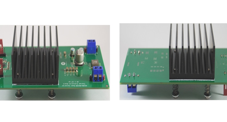
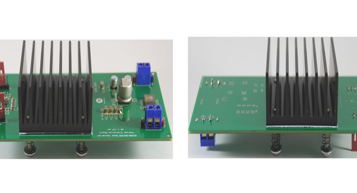
Figure 3: Test board with TSC (left) and BSC (right)
Measured Results
For this test setup, only a slight difference (
30°C lower with the 60 mm heat sink
15 to 20°C lower with a 25 mm heat sink
10°C lower with a 10 mm heat sink
The results show that TSC MOSFETs with a heat sink enable similar thermal performance to BSC MOSFETs mounted on a thermally optimized PCB with low density of surrounding components. However, where minimizing heat flows into the PCB is required, MOSFETs with a top-side exposed pad are the right choice, as the thermal resistance to the heat sink mounted on the top side of the package is lower.
Benefits Beyond Cooling
onsemi provides TSC MOSFETs for automotive applications like NVMJST0D9N04C, which are housed in a TCPAK57 package measuring just 5mm x 7mm. These devices feature a 16.5mm2 thermal pad on the top side, dissipating heat directly into a heatsink rather than the PCB. By enabling the use of both sides of the PCB and decreasing the amount of heat going into the board, the TCPAK57 package enables increased power density, better reliability, and an overall extended system lifetime.
You May Also Like

.jpg?width=300&auto=webp&quality=80&disable=upscale)

