November 7, 2011

A new production technique using superionic glass could lead to tiny, integrated diagnostic sensor arrays on surfaces as small as a square centimeter, fuel cells to power microelectromechanical systems (MEMS), and faster, more reliable optical micro-gyroscopes.
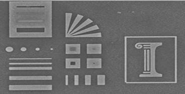
Nicholas Fang, associate professor of mechanical engineering at MIT, and colleagues at the University of Illinois at Urbana-Champaign have developed a more precise engraving technique that etches tiny, nano-sized patterns on metallic surfaces using a small, voltage-activated stamp made out of glass.
The technique could be used to produce "lab-on-a-chip" designs that let clinicians perform tests for hundreds of diseases, such early-stage cancers, from a single drop of blood. Each tiny dot on the engraving, one hundredth the width of a human hair, could act as an optical antenna tuned to the specific wavelength of a single molecule.

Because the engraving technique can produce patterns of dots just 30 nanometers wide at a higher resolution than nanoimprint lithography, it greatly increases the surface area of a minuscule piece of metal, Fang says. This could reduce the amount of platinum necessary to produce the MEMS devices that power the insect robots used for military surveillance.
"This is a very important aspect if you want to reduce the amount of catalyst being used in different power sources such as fuel cells," he explains. "For example, the amount of platinum used in MEMS fuel cells already is a big concern. If you can lower the use of platinum while keeping the device as efficient, you can lower the cost."
The new process uses superionic glass, which is composed partly of ions that can be electrochemically activated when pumped with voltage. The molten glass is pressed on to a master pattern, forming a mold that's pressed on to a flat silver substrate. When a 90-millivolt electric potential is applied above the silver layer, the voltage stimulates ions in both surfaces, triggering the glass mold to etch into the metal substrate.
For the electrochemical stamping process, "we need something almost like a sponge that contains moving ions," Fang says. "Ions in the glass move almost as quickly as they do in a liquid."
In the abstract for the research paper, the authors wrote:
This paper demonstrates and analyzes the new use of the glassy solid electrolyte AgI-AgPO3 for direct nanopatterning of thin silver films with feature resolutions of 30 nm. AgI-AgPO3 has a high room temperature ionic conductivity with Ag + as the mobile ion, leading to silver etch/patterning rates of up to 20 nm s -1 at an applied bias of 300 mV. The glass can be melt-processed at temperatures below 200 degrees C, providing a facile and economical pathway for creating large area stamps, including the 25 mm2 stamps shown in this study. Further, the glass is sufficiently transparent to permit integration with existing tools such as aligners and imprint tools, enabling high overlay registration accuracy and facilitating insertion into multi-step fabrication recipes.
The use of glass as a stamp was counterintuitive, Fang says. "Our impression is that glass is fragile, and it's hard to use it to pattern on to something. But at a nano scale, it tends to be more reliable than we thought."
For proof of concept, the researchers filled a small syringe with glass particles and heated the needle to melt the glass inside before casting it into the mold. Now, they've created a small lab foundry with an interior of approximately one cubic foot.
"It's almost like an ice cream machine, where you push ice cream out of a jet," Fang says.
To scale up to full production, the researchers hope to transfer the patented technology to an outside company or spin it off in a student-led startup. Fang says the group could be ready to produce millions of chips within a year. To get there, he estimates the needed capital investment would be less than $30 million.
Such a company could piggyback on developments in glass technology in the past decade used to produce the larger sheets of stress-free glass used in flat-panel TVs and monitors.
The challenge is not only to develop commercial-grade glass foundry tools but also to find a niche application to attract a particular sector. For example, the technique could be used to replace the mechanical MEMS gyroscopes used in mobile phone accelerometers with potentially faster and more reliable optical micro-gyroscopes.
About the Author(s)
You May Also Like


