Want to Learn about PCB Fab, Optical Transceivers, and Power Integrity?
Learn from experts during the DesignCon five-session complimentary webinar series!
April 15, 2021

This week kicks off a five-session complimentary webinar series featuring experienced engineers from DesignCon’s conference program, including experts from Keysight Technologies, Intel, Picotest, NXP, Lamsim Enterprises, and VSI Labs. These technical veterans are sharing practical insights and knowledge to design the next generation of technologies.
You can register for any of the sessions here. If you can’t make all the sessions, don’t worry! All of them will be available for viewing after each session. Now let’s look at what’s been covered in the first few days of the webinar series.
PCB Fabrication for SI/PI Engineers
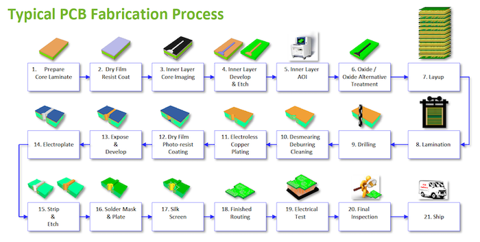
Lambert (Bert) Simonovich, President of Lamsim Enterprise, provided important guidelines that signal integrity (SI) and power integrity (PI) engineers need to know when doing first-time modeling for PCB fabrication. He talked about conductor roughness, phase delay, and insertion loss, including the use of the Cannonball-Huray roughness model and how to apply it in several EDA software tools. Simonovich also covered how to extract and apply the right material properties from manufacturers’ data sheets to use for high-speed channel modeling. He wrapped up his discussion by listing the advantages and pitfalls of PCB stackup on power integrity.
For reference, a PCB stackup drawing is the first step in the fabrication process. A poorly designed stackup and lack of detailed fabrication notes can result in degraded signal & power integrity, manufacturability, and reliability of the finished product. Often SI/PI engineers make wrong design assumptions, leading to inaccurate modeling and simulation results. Because of this, they need to understand the PCB design and fabrication nuances to avoid pitfalls in achieving useful first-time models.
Optical Transceiver Design
Hyper-scale data centers (HSDC) typically require millions of optical transceivers, creating a huge demand for 400G/800G products. The exponential growth in data communication driven by HSDC due to cloud computing, cloud storage, Augmented Reality (AR), Virtual Reality (VR), Video on Demand (VoD), 5G, Internet of Things (IoT), and autonomous driving are the dictating factors for much higher bandwidth and lower power consumption.
Optical transceiver design is a complex process as it requires multiple disciplines such as electrical, mechanical, optical, and firmware to come together precisely to provide the required electro-optical performance. The designer faces significant challenges in the design of 800-Gbps transceivers due to their form factor, high speed, high power consumption, and channel density. Now that 800-Gbps transceivers are in their early sampling stage, the optical industry has already started the discussion on the next generation of optical transceivers providing a bandwidth of 1.6 Tbps and 3.2 Tbps.
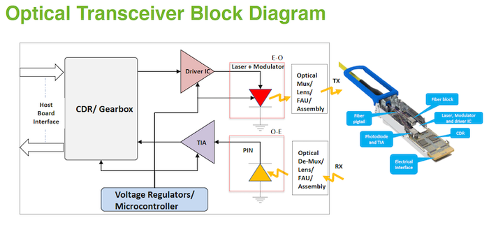
Designing these new generations of transceivers will require a much higher level of integration and many technological and packaging breakthroughs. In preparation for this technology, engineers need to understand the basics of optical transceivers and discuss the design consideration of 400-Gbps, 800-Gbps, and next-generation transceivers.
Two experts from Intel provided a good introduction to these fundamentals. Sunil Priyadarshi Director, Intel, and Sanjeev Gupta, Principal Engineer and R&D Manager, Intel, started their talk with a review of the basics of optical transceivers. Much of their discussion then focused on the design considerations for 400/800-Gbps transceivers, including the benefits of co-packaged optics to achieve improved system-level power reduction vs. front plate pluggable and with power-optimized SerDes for in-package chip-to-OE channel
Impedance Tips to Improve Power Integrity
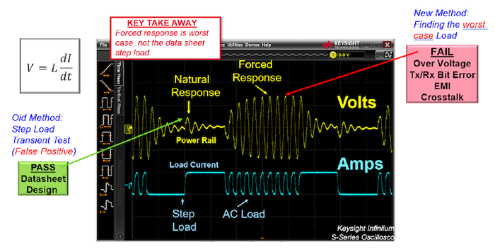
Power Integrity is all about delivering the appropriate power to maintain the signal integrity (SI) of dynamic loads, all with power delivery design margins that allow for reliable product performance. The key challenge for the PI engineer is that the dynamic load can operate from DC to GHz, resulting in extreme bandwidths of power delivery and the potential for EMI. Target Impedance vs. frequency is a great tool for designing for power delivery over the full bandwidth of the dynamic load, but designers often fail to realize its full benefit
Heidi Barnes, SI and PI Applications Engineer at Keysight Technologies, and Steve Sandler, Founder, and President, Picotest.com, shared useful technical insights into how to reverse engineer target impedance to generate requirements for the VRM’s active inductance and the load’s package/die capacitance. They encouraged engineers to follow flat impedance design techniques to improve design margins over component tolerances and avoid the disaster of a rogue voltage wave arriving at the load. Finally, they explored advanced PI ecosystem time-domain simulations with EM PCB models to understand Power Supply Rejection Ratio (PSRR) and the potential sources for conducted EMI.
The following are still to come up this week:
Thursday, April 15, 2021, 1:00 p.m. EDT: "Controlling the Waves: A Field-based Perspective on High-speed PCB Design," by Daniel Beeker, Senior Principal Engineer, NXP
Friday, April 16, 2021, 1:00 p.m. EDT: "OEM Roundup 2021: The New ADAS," by Danny Kim, Director of Advisory Services, VSI Labs
In addition to the free webinar sessions, attendees will also have the opportunity to enjoy a networking session at the close of the week with select speakers from DesignCon’s conference, where they can meet with fellow attendees, set up one-on-one meetings, and get to know industry peers.
Don’t worry if you missed a few of the sessions. They will be available on-demand for viewing. Plus, attendees of the Spring Break Webinar can also look forward to receiving a discount code to attend DesignCon’s annual in-person conference set to take place at the San Jose McEnery Convention Center, August 16-18, 2021.
John Blyler is a Design News senior editor, covering the electronics and advanced manufacturing spaces. With a BS in Engineering Physics and an MS in Electrical Engineering, he has years of hardware-software-network systems experience as an editor and engineer within the advanced manufacturing, IoT and semiconductor industries. John has co-authored books related to system engineering and electronics for IEEE, Wiley, and Elsevier.
About the Author(s)
You May Also Like


