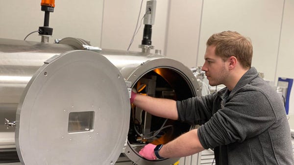
‘Shaving' Nanocrystals Can Improve Electrical Conductivity
Researchers find a way to reduce materials gaps that can allow for the creation of materials for future advanced electronic devices.
April 7, 2022

For the development of next-generation electronics—which will be not only more powerful but likely more flexible and even smaller—researchers need new materials. Ones that shows promise for this purpose in part because of their ability to be grown from many different materials—including metals, semiconductors, and magnets—are nanocrystals.
However, historically, whenever scientists have assembled these nanocrystals together into arrays, the newly formed “supercrystals would grow with long “hairs” around them, which hinders electron flow and rendered them unsuitable for electronic applications.
Now a team from the University of Chicago has figured out how to atomically “shave” the hairs to facilitate more electrical collaboration between groups of nanocrystals, paving the way for their use in novel devices with advanced capabilities.
Indeed, researchers call nanocrystals “super atomic building blocks” for their property of granting new abilities--for example, letting cameras see in the infrared range, said University of Chicago Professor Dmitri Talapin, one of the researchers and a senior scientist at the Department of Energy’s Argonne National Laboratory.
“But until now, it has been very difficult to both assemble them into structures and have them talk to each other,” he said. “Now for the first time, we don’t have to choose. This is a transformative improvement.”

Observing Atomic Processes
To come up with a solution to shave the hairs so they could pack the nanocrystals more tightly together and reduce any gaps between them, researchers first had to observe them at the atomic level.
To do this, researchers used X-rays at the Center for Nanoscale Materials at Argonne and the Stanford Synchrotron Radiation Lightsource at SLAC National Accelerator Laboratory, as well as conducted simulations and models of the chemistry and physics at play within the materials.
“When these gaps are smaller by just a factor of three, the probability for electrons to jump across is about a billion times higher,” Talapin explained in a press statement. “It changes very strongly with distance.”
What they discovered during their observations was that during the process to grow the supercrystals—part of which is done in a liquid solution—the material goes through a unique transformation in which gas, liquid, and solid phases of it all coexist.
By controlling the chemistry of this stage in a precise way, researchers could create crystals with harder, slimmer exteriors that could be packed in together much more closely, said Josh Portner, a Ph.D. student in chemistry who also worked on the research. “Understanding their phase behavior was a massive leap forward for us,” he said.
Potential Applications
Through their work, researchers were able to develop design rules which should allow for the creation of many different types of nanocrystal materials that maintain the electrical conductivity needed for advanced electronic devices.
The team published a paper on its work in the journal Science. Though the full range of applications for their work remains unclear, the scientists envision a number of areas where their technique could be useful.
“For example, perhaps each crystal could be a qubit in a quantum computer; coupling qubits into arrays is one of the fundamental challenges of quantum technology right now,” Talapin said.
Further exploration of unusual intermediate state of matter seen during the growth of the supercrystals also is rare, and could provide clues for chemists in how to build other types of new materials in the future, Portner added.
Elizabeth Montalbano is a freelance writer who has written about technology and culture for more than 20 years. She has lived and worked as a professional journalist in Phoenix, San Francisco, and New York City. In her free time, she enjoys surfing, traveling, music, yoga, and cooking. She currently resides in a village on the southwest coast of Portugal.
About the Author(s)
You May Also Like


