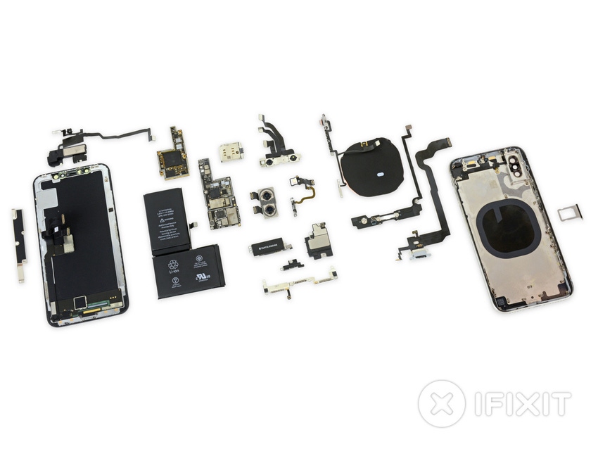
What's going on inside the iPhone X to justify that hefty $1000 price tag? An iFixit teardown reveals some clever, old-school engineering to pack a lot technology into a small space.
November 10, 2017

Look ma, no Home button!
With the iPhone X Apple has gone for more than fancy Roman numeration in the name. The new flagship smartphone is the first to feature an exterior that has no buttons or framing. This phone's front is all-screen, specifically a 5.8 inch OLED multitouch Super Retina HD display with 2436 × 1125-pixel resolution (458 ppi). The iPhone X also features dual 12-megapixel cameras, a 7-megapixel TrueDepth camera for video and the phone's new facial recognition unlock feature (Face ID), and support for Qi wireless charging.
 Ten years since the release of the first iPhone, the team at iFixit decided to take a look inside of the “glass sandwich” and revealed some engineering work that harkens back to the very early days of the smartphone.
The iPhone X shares some hardware with the iPhone 8 and 8 Plus, such as the Qualcomm modem and LTE transceiver. The most notable bit of shared hardware is Apple's highly touted new A11 Bionic chip, which is optimized for emerging applications such as machine learning and augmented reality.
A11 chip aside, where Apple put in some real engineering know-how into the iPhone X is in its space-efficient logic board. According the iFixit, the iPhone X has less bare board than even an Apple Watch and makes the iPhone 8 Plus' board look “gangly and expansive” by comparison, all while packing in more tech. The iPhone X's motherboard takes up about 70% of the footprint of the iPhone 8 Plus' by iFixit's estimation.
Can you fix modern electronics? Or have manufacturers put an end to electronics repair? In this keynote presentation at ESC Silicon Valley, taking place Dec. 5-7, 2017, Kyle Wiens, CEO of iFixit, will discuss the Right to Repair as he tears down Apple's iPhone X, uncovering its cutting-edge AR (augmented reality) sensor, and compares it to the competition while discussing the tradeoffs and decisions made by Apple's product designers. Click here for more information on Kyle's talk. Click here to register for the event today! |
Apple engineers accomplished this feat by folding the board in half and soldering the two halves together, with the A11 chip nestled in the middle. Taken separately iFixit estimates the board layers of the iPhone X would take up to 135% of the iPhone 8 Plus' logic board area. Interestingly this is the first time Apple has done this since the release of the very first iPhone. Maybe the engineers decided to employ some throwback techniques in honor of the iPhone's anniversary? You can't argue with the results. To make all of this work the two layers have a third printed circuit board spacer between them, and instead of connecting the layers with flex cable Apple's engineers opted to use vertical interconnect access (vias) to allow data transfer using through-holes.
Here's a breakdown of the logic board components:
|
Apple engineers saved space in the iPhone X by folding and layering the logic board (image source: iFixit). |
On the first half:
Apple APL1W72 A11 Bionic SoC layered over SK Hynix H9HKNNNDBMAUUR 3 GB LPDDR4x RAM
Apple 338S00341-B1
TI 78AVZ81
NXP 1612A1—Likely an iteration of the 1610 tristar IC
Apple 338S00248 audio codec
STB600B0
Apple 338S00306 power management IC
Apple USI 170821 339S00397 WiFi / Bluetooth module
Qualcomm WTR5975 gigabit LTE transceiver
Qualcomm MDM9655 Snapdragon X16 LTE modem and PMD9655 PMIC
Skyworks 78140-22 power amplifier, SKY77366-17 power amplifier, S770 6662, 3760 5418 1736
Broadcom BCM59355 touch controller
NXP 80V18 PN80V NFC controller module
Broadcom AFEM-8072, MMMB power amplifier module
And on the outside of the logic board sandwich:
Toshiba TSB3234X68354TWNA1 64 GB flash memory
Apple/Cirrus Logic 338S00296 audio amplifier
Overall iFixit gave the iPhone X a repairability score of 6 out of 10. Display and battery repairs are easy and a cracked display can be replaced without removing the Face ID hardware. But the double-stacked logic board makes board-level repair nearly impossible. The glass exterior also makes the phone prone to damage if dropped and if the back glass breaks it will require removing every component and replacing the entire chassis to fix.
Check out the full iFixit teardown below and join Design News at ESC Silicon Valley for a live Apple iPhone X teardown and discussion.
Chris Wiltz is a senior editor at Design News, covering emerging technologies including VR/AR, AI, and robotics.
[all images courtesy iFixit]
About the Author(s)
You May Also Like


