Ode to Bodacious Breadboards, Part 1
There’s a lot more to breadboards than meets the untrained eye.
March 8, 2024
At a Glance
- In addition to attaching multiple breadboards together, it’s also possible to detach power/ground rail sub-assemblies
- Some breadboards have split power/ground rails, supporting multiple voltages (e.g., +12V, 0V, & –12V or +5V, +3.3V, & 0V)
It’s a funny old world and no mistake. It’s a truism that if you know something yourself, then you often tend (sometimes incorrectly) to assume that everyone else knows it, too, especially if it relates to a topic you share in common, like electronics, for example.
Take the humble breadboard as a case in point. I know that newcomers to electronics are often unfamiliar with these little rascals. However, I�’ve been surprised twice in the past couple of days when professional engineers have asked me breadboard-related questions about something I would have assumed they already knew, like, “Why aren’t I seeing +5 V power on both sides of my breadboard?”
Even if you do consider yourself to be au fait with breadboards, I’d love to hear from you if—upon perusing and pondering this column—you discover something that makes you say something like, “Well, blow me down with a feather, I never knew that!” (If so, please feel free to email me at [email protected].)
Let’s start with the old chestnut as to the origin of the breadboard moniker. Way back in the mists of time, up until the 1960s, radio amateurs and electronic hobbyists often hammered nails into a wooden board and then soldered their components and wires to these nails. In the case of younger members and newcomers to the game, it wasn’t uncommon for them to employ the breadboard (the board upon which the family’s bread was sliced) from the kitchen. (My mother was less than pleased, let me tell you!)
When breadboards of the type we know and love today first appeared on the market, they were referred to as “solderless breadboards” to distinguish them from the other kind. Over the years, as memories began to fade, we dropped the “solderless” part as being superfluous to requirements.
Breadboards are available in all shapes and sizes, the two most common being the half-size (with 300 signal tie points and 100 power and ground tie points) and full-size (with 630 signal tie points and 200 power and ground tie points) as illustrated below.
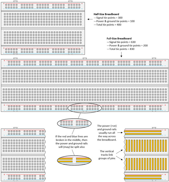
Half- and full-sized breadboards. CLIVE "MAX" MAXFIELD
Although this is a personal choice, when I’m working with breadboards, I always orient them as shown in this diagram—that is, with the red power rail at the very top. The lower right-hand side of this image shows the conducting connections inside the breadboard.
One very important point to note relates to the power and ground rails, which span the board (or not, as the case might be). Some breadboards have these rails split in the middle, which makes them useful in those cases when you wish to employ multiple voltages, like +12 V, 0 V, and –12 V for analog circuits with operational amplifiers (opamps), or +5 V, +3.3 V, and 0 V if you are mixing different microcontrollers and sensors. The potential “gotcha” is that the red and blue lines spanning the board may or may not have breaks in them to indicate the split nature of the breadboard.
The first time you are caught unaware by this, it can result in a “bad hair day” while you attempt to track down your problem. It’s said that you learn from your mistakes. Personally, I prefer to learn from other people’s mistakes. In this case, you can learn from my mistakes (you’re welcome).
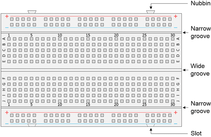
Meet the nubbins. CLIVE "MAX" MAXFIELD
Sometimes a single breadboard isn’t enough. If you flip your breadboard over and look carefully, what you originally assumed to be a simple card backing turns out to have adhesive on both sides. One side is attached to the bottom of the board. If you peel away the protective layer on the outward facing side, you can attach your breadboard to a larger surface.
Also observe that each board has protruding nubbins on one side and corresponding slots on the other (some boards also have them on the ends). These facilitate joining multiple boards together.
One thing that tends to take a lot of people by surprise is when they come to learn that the narrow grooves between the center of the board and the power/ground rails at the top and bottom of the board aren’t there for aesthetic purposes only. If you use a sharp knife to cut through the backing on the bottom of the board in a line corresponding to one of these narrow grooves, you’ll discover that the matching power/ground sub-assembly is attached to the main board by its own nubbins or slots.
Observe the ‘A’, ‘B’, ‘C’… annotations at the sides of the board. Also, the numerical annotations ‘1’, ‘5’, ‘10’… at the top and bottom of the board. These allow people to communicate valuable information to each other, like “Connect a 100-Ω resistor between E5 and F5.” Based on this, you might assume it would make sense for all breadboards to be as shown in the image above; that is, with the letters on the left-hand side of the board corresponding to those on the right, and the numbers on the top of the board matching those on the bottom. “Oh, you poor innocent,” is all I can say.
I was just reading the March 2024 issue of Practical Electronics, which is the UK’s premier computing and electronics hobbyist magazine (in addition to the UK, PE is available worldwide, both in print and via PDF download). They’ve just launched a new Teach-In series: Learn electronics with the ESP32 by Mike Tooley. I was particularly interested to see the first breadboard image as shown below.
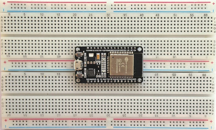
Dual breadboard setup. MIKE TOOLEY/PRACTICAL ELECTRONICS, ELECTRON PUBLISHING)
Multiple points of interest immediately pop out to me. How about you? Do you see anything you might be tempted to use as a “teachable moment”?
First, observe the width of the ESP32 module. If we mounted this straddling the wide groove in the center of a single breadboard, it would span rows ‘A’ to ‘I’ (or ‘B’ to ‘J’), which would make it hard to connect the pins on one side of the module to anything else. This is why Mike has it straddling a brace of breadboards. To achieve this, however, he’s removed the upper set of power/ground rails from the lower breadboard.
Speaking of the power/ground rails, observe that the red and blue lines have breaks in the middle, thereby indicating that these breadboards are of the split rail flavor (in later images, Mike’s added jumper wires at these points).
Anything else? How about the fact that the numerical annotations start at ‘0’ instead of ‘1’? Also, that the ‘0’ starts one column in from the edge, which would make the number of the left-most column ‘–1’. Even better (or worse, depending on your point of view), the numerical annotations associated with the columns are mirror-imaged between the top and bottom of the board. Similarly, for the ‘A’, ‘B’, ‘C’ annotations associated with the rows at the ends of the board. This means that implementing an instruction like “Connect a 100-Ω resistor between E5 and F5” is problematic because there are two possibilities.
There’s so much more I want to talk about (much like my dear old mother, the real trick is to get us to stop talking), but I fear this column is long enough already, so we’ll save my remaining meandering musings until next time. Until that frabjous day, I welcome your insightful comments, penetrating questions, and sagacious suggestions.
About the Author(s)
You May Also Like


