New modular robots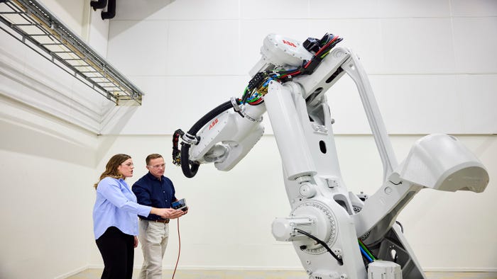
AutomationABB Expands Its Modular Large Robot PortfolioABB Expands Its Modular Large Robot Portfolio
ABB’s new IRB 7710 and IRB 7720 robots offer new levels of flexibility and greater choice with almost 50 variants.


.jpg?width=700&auto=webp&quality=80&disable=upscale)


.png?width=300&auto=webp&quality=80&disable=upscale "Q&A")


 Closure device.")
Editors' Choice

.jpg?width=300&auto=webp&quality=80&disable=upscale)

Jun 4 - Jun 6, 2024
Jun 4 - Jun 6, 2024
Innovation in automation starts here. Discover and collaborate on automation solutions that are revolutionizing the entire production lifecycle — from design to production to market — and sharpen your competitive edge. ATX South is part of IME South, a six-in-one expo offering the latest insights & solutions spanning medtech, packaging, automation, plastics, design, & processing.
Register NowSign up for the Design News Daily newsletter.