Bosch is Gunning for a Bigger Slice of the Automotive Semiconductor Business
Bosch’s new 300-mm silicon wafer fab employs the larger 40-200 nm lithography automotive customers need.

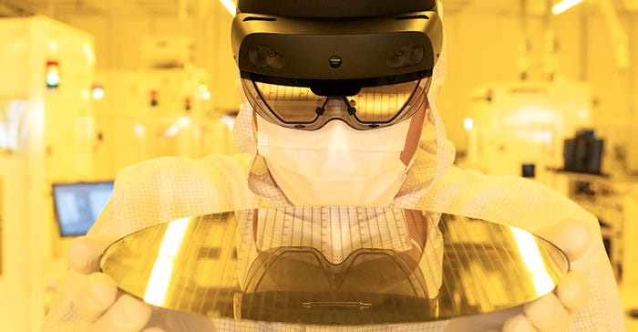
Workers in Bosch's Dresden plant use augmented reality glasses and tablets to see digital content superimposed on the real environment.Image courtesy of Bosch
The global automotive semiconductor market is forecast to reach $73.2 billion by 2028, with a compound annual growth rate of 11.5 percent from its $38.1 billion level in 2021. That’s according to a new report from Vantage Market Research.
Bosch aims to participate in this booming market, with a 3 billion Euro investment in its semiconductor division, which has recently opened a new 300-mm silicon wafer fab in Dresden. “Microelectronics is the future and is vital to the success of all areas of Bosch business,” observed Dr. Stefan Hartung, chairman of the Bosch board of management during Bosch Tech Day 2022. “We’re gearing up for continued growth in demand for semiconductors – also for the benefit of our customers,” Hartung said. “For us, these miniature components mean big business.”
Bosch says it is targeting technologies such as systems-on-a-chip and radar sensors, aiming to make them smaller, smarter, and cheaper to produce. Recognizing the risk of lengthy supply chains, Bosch says it is supporting an effort to double Europe’s slice of global semiconductor production from 10 to 20 percent by the end of the decade. “Europe can and must capitalize on its own strengths in the semiconductor industry,” Hartung said.
A key factory in automotive semiconductor shortages that have plagued OEMs is the industry’s use of larger-scale 40-to-200-nanometer semiconductor lithography than is employed by the latest computers and consumer electronics. Bosch’s facilities will produce chips at this larger scale, according to Hartung. “More than ever, the goal must be to produce chips for the specific needs of European industry,” he said. “And that means not only chips at the bottom end of the nanoscale.”
The company is expanding another semiconductor center in Reutlingen, spending 400 million Euros on it by 2025. This will expand its manufacturing capacity and convert of existing factory space into new clean-room space. A new 3,600-square-meter extension in Reutlingen, which will contribute to the facility’s clean room expansion from today’s 35,000 square meters to more than 44,000 square meters by the end of 2025.
The Dresden 300-mm fab boasts an array of technical features designed to put it on the cutting edge of chip manufacturing. This includes the connection of all the roughly 100 machines and lines in the 10,000-square-meter cleanroom so they can communicate with each other and with the building’s infrastructure.
That required 300 kilometers (186 miles) of data lines carrying as many as 1,000 data channels for each machine in real time and relaying it to a server in the plant.
In total, the production data generated is equivalent to 500 pages of text per second, equaling more than 42 million pages per day. Within this avalanche of data is information on the status of where each individual wafer is in the production process, where it is going next, and when it will arrive. The wafers are transported from machine to machine by a completely automatic system featuring individual pods known as FOUPs (front opening unified pods). Each FOUP can transport as many as 25 wafers, so the factory doesn’t need any manual transportation of wafers at all.
That mountain of data can’t be monitored manually, so that is automated too, with an AI evaluating the data generated in the wafer fab to detect even the tiniest anomalies in products. These anomalies are visible on the wafer surface in the form of specific error patterns known as signatures. Their causes are immediately analyzed and deviations from the process corrected without delay, even before they can affect the reliability of the product.
Bosch says that this is the key to further improving the manufacturing processes and semiconductor quality, as well as to achieving a high level of process stability. It also means that semiconductor products can go into full-scale production quickly.
Additionally, the AI’s algorithm predicts when a piece of manufacturing machinery or a robot needs maintenance or adjustment, so such work is not done according to a rigid schedule, but only when it is needed before any problems arise.
One way the plant is kept running smoothly is by modeling its operations with a digital twin. During construction, all parts of the factory and all relevant construction data relating to the plant were recorded digitally and visualized in a three-dimensional model.
The resulting digital twin comprises roughly half a million 3D objects, including buildings and infrastructure, supply and disposal systems, cable ducts and ventilation systems, and machinery and manufacturing lines. This allows Bosch to simulate both process optimization plans and renovation work without intervening in ongoing operations.
It isn’t only the machinery that is augmented with connected data. The plant’s workers employ augmented reality using smart AR glasses and tablets to see digital content superimposed on the real environment. One AR app developed by Bosch displays energy data from the wafer fab in a virtual model of the building to optimize the efficiency of the manufacturing machinery. Another app uses glasses to help with construction planning and another is planned to aid remote maintenance of the plant’s machinery.
Meanwhile, the Reutlingen plant is gearing up to make silicon carbide semiconductors for high-voltage EV power electronics. Bosch has been mass-producing silicon carbide chips since the end of 2021. Because silicon carbide can contribute to a hard-won 6 percent increase in driving range this market is seeing annual rates of 30 percent or more, according to the company.
Bosch is investigating even more exotic technology for EV applications. “We’re also looking into the development of chips based on gallium nitride for electromobility applications,” Hartung said. “These chips are already found in laptop and smartphone chargers.” To make these chips suitable for power electronics in EVS they will have to become more robust and able to withstand substantially higher voltages of up to 1,200 volts.
“Challenges like these are all part of the job for Bosch engineers,” Hartung added. “Our strength is that we’ve been familiar with microelectronics for a long time – and we know our way around cars just as well.”
This is true, as Bosch has been active in automotive electronics for more than 60 years. The Bosch semiconductor plant in Reutlingen, for example, has been producing chips based on 150- and 200-millimeter wafers for the past 50 years. With the recent investments, it seems like both of Bosch’s semiconductor sites are well-positioned for the next 50 years.
About the Author(s)
You May Also Like


