Performance-Tuning Arm-Based SoC Designs
A forthcoming book promises to bring smiles to the faces of Arm-based system-on-chip (SoC) designers.
October 18, 2023

Just to get the ball rolling, let’s start by reminding ourselves that system-on-chip (SoC) devices are composed of functional units called intellectual property (IP) blocks or cores. A modern SoC can be composed of hundreds of IPs, many of which may contain hundreds of millions of transistors. In fact, even relatively small startup companies can create multi-billion transistor devices these days without raising so much as a quizzical eyebrow from the metaphorical market.
It’s common for design teams to purchase multiple IPs from various vendors, to “stitch” these IPs together, and to be surprised (horrified) when the system fails to meet its performance goals. And when I say, “fails to meet its performance goals,” I’m not talking about being 5% below par. I know of one company that created a relatively simple SoC in the scheme of things. This device was primarily composed of multiple processor IP cores from one vendor and multiple memory controller IP cores from another vendor. The team thought everything was going to be easy peasy lemon squeezy, all the way until they received first silicon back from the foundry, at which point they discovered they were achieving only 50% of the theoretical maximum bandwidth between the memory controller and the memory.
This is where the finger-pointing began. The design team had no realistic way to analyze what was going wrong, so they threw the support burden back on their IP suppliers. At the end of the day, it turned out that the memory controller had not been configured in such a way as to handle the workload characteristics specific to the applications running on this design. Fortunately, the fix was relatively easy in this case, but the device didn’t reach the market until it was way behind schedule.
If you are involved in designing Arm-based SoCs, then I’m about to make you very happy indeed. I’m poised to tell you about something that will allow you to optimize and performance-tune your designs to achieve the maximum data throughput for your application workloads. First, of course, we need to set the scene…
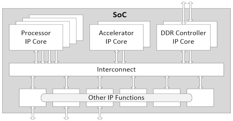
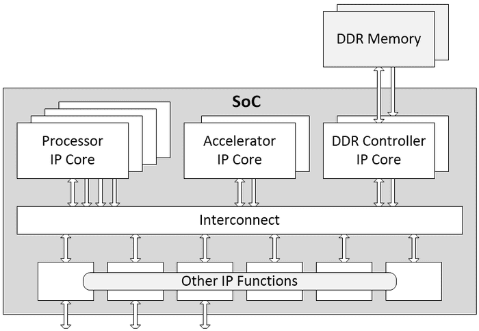
If we take a 30,000-foot view of an SoC, we might expect to see one or more processor cores, one or more hardware accelerator cores, and one or more memory controllers to communicate with external memory, which is typically presented in the form of double data rate synchronous dynamic random-access memory (DDR SDRAM), or just DDR for short. Also, there will be additional functions like an interrupt controller, some general-purpose input/outputs (GPIOs), a real-time clock (RTC), and a boot controller, but let’s not worry about these additional functions too much here.
Many of these IPs will be acquired from trusted third-party vendors. For example, the processor core IPs often come from Arm, while any DDR memory controller IPs may originate with Cadence Design Systems. Meanwhile, the hardware accelerator IPs for functions like artificial intelligence (AI) and machine learning (ML) will typically be designed in-house. These accelerator IPs provide the “secret sauce” that will differentiate this SoC from competitive offerings.

In the not-so-distant past, the interconnect was a simple bidirectional bus and the IPs themselves were also relatively unsophisticated. Reading and writing to locations in the external memory was also an uncomplicated, time-deterministic process. In those days, the system’s performance was dictated by the processor’s architecture, the processor’s clock speed, and the memory system to which the processor was connected. Increasing the clock frequency resulted in higher performance. Like Pooh, I’m a bear of little brain, but even I could wrap my brain around this.
At that time, the performance of a new system was relatively easy to predict, and only small amounts of optimization and analysis were required. By comparison, today’s interconnects are sophisticated chip-spanning IPs in their own right. For example, consider Arm’s Advanced Microcontroller Bus Architecture specification (AMBA). Amongst other things, AMBA encompasses the Advanced eXtensible Interface (AXI), which is a non-cache coherent on-chip communication bus protocol, and the Coherent Hub Interface (CHI), which enables multiple cores to share data in a cache coherent manner.
Meanwhile, the cores themselves are becoming larger and more complex, with each new generation featuring longer and longer execution pipelines in order to improve their performance. Also, all of today’s IP cores are incredibly configurable and support myriad use models.
Speaking of use models, each system use case can involve a different mix of application workloads. In turn, these workloads generate memory traffic patterns that are combined by the interconnect through caching systems—where copies of memory can be shared—into a blended memory access stream. Predicting what this stream will look like is tricky, to say the least. Also, the behavior of the processor subsystem infrastructure under these traffic loads is hard to predict.
The bottom line is that the complexity of the processors and accelerators, the multiplicity of memory controllers, the increasing use of multi-level cache subsystems, and the ability to configure all aspects of the system mean that accurately predicting system performance has become significantly more difficult. This is unfortunate because, at the same time, accurately predicting system performance has become increasingly important.
The problem is that a lot of today’s newcomers to SoC design are under the impression that all they need to do is stitch IPs together like LEGO blocks. It’s not uncommon for even an experienced design team to progress all the way to receiving first silicon, only to discover that their real-world workloads are achieving only a fraction of the anticipated data throughput.
This is where the finger pointing starts. First, the designers accuse the processor IP vendor of providing a core that doesn’t meet its data sheet specifications. “No way,” replies the processor supplier, pointing to benchmark results that back their case. Next, the designers direct their ire toward the DDR controller IP vendor. “Not our fault,” replies the supplier, “Our controller has a proven track record in numerous real-world designs.”
At the end of the day, it almost invariably turns out that the designers of the SoC have not configured the various IPs correctly in the context of the workloads with which they are being tasked.
Let’s stick with the DDR memory and the DDR controller as one example where problems can occur. To be honest, I find it hard to wrap my brain around all of this but let me try to summarize things as follows. At the heart of a DDR memory chip, we have a cell that can store a single bit of data. This is essentially an analog device that doesn’t get significantly faster when we move to more advanced process nodes.
There’s a mindbogglingly complex hierarchy above the level of an individual cell that involves rows, columns, pages, banks, and bank groups, and these are just inside the DDR chip. Multiple DDR chips are gathered into ranks forming a module, and these ranks are addressed by channels from the memory controller. All of this provides multidimensional parallelism that can be exploited to increase the speed of the memory.
Performing a single operation like reading or writing a word of data takes quite a long time in the scheme of things (don’t ask me what I mean by “word,” because neither of us would be happy with my answer—I’m just trying to build a picture here). It’s also not possible to generate a subsequent read or write to a location close to the original location until the first transaction has completed. However, it is possible to generate an overlapping series of reads or writes to locations that are sufficiently far away from each other in the memory map. In this case, although the individual read and write operations are relatively slow, the time for a series of such operations is very fast indeed.
A DDR memory chip itself is designed to be cheap-and-cheerful but not very clever. All the “smarts” are implemented by the memory controller and the processor and accelerator cores. As an example, the controller can be instructed (configured) to implement a logical to virtual address mapping algorithm. What this means is that, while the programmer and the program visualize the memory as a linear sequence of locations starting at 0 and working their way up, the controller implements a logical to virtual address mapping algorithm to spread operations through the memory map.
Of course, it would be unfortunate if the application software were to perform some task, like accessing every 1024th word in an array, where this just happened to clash with the controller’s logical to virtual address mapping algorithm, thereby slowing the system to a crawl. Happily, the controller can be configured to perform a wide variety of mapping algorithms. Sadly, the SoC designers won’t even know there’s a problem until it’s too late… unless they have some way to model what was happening.
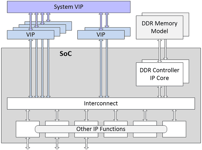
SoC designers and verification engineers have long used the concept of Verification IP (VIP). These are IP blocks that can be inserted into the testbench to evaluate interfaces and protocols. They do this by converting the high-level transactions used by the verification environment into the low-level “bit-twiddling” required by the design being verified.
What the folks at Cadence have done is to create something called System VIP that conceptually “sits on top” of the regular VIP. Take the example SoC we were talking about before. Just one of many possible scenarios might be as represented below.

In this particular scenario, the System VIP can be used to replicate the types of workload traffic patterns that are expected to be generated and consumed by the processor and accelerator cores. All of this is accompanied by a System Performance Analyzer (SPA) tool that provides the ability to analyze the results from simulation or emulation runs. The SPA utilizes transaction details to provide sophisticated splitting, filtering, and other powerful analysis features that help debug what is happening when a bandwidth drop-off or latency spike occurs. These insights allow the designers to configure the various IPs to achieve optimal performance for their application workloads.
I could waffle on about this for hours. Happily, I don’t need to do so because Nick Heaton from Cadence and Colin Osborne from Arm are writing a book about this: Arm Performance Cookbook: Understanding and Optimizing the Hardware Performance of Arm-Based SoCs.

All my friends who are working in this arena are tremendously excited about this and there’s a growing buzz in SoC space (where no one can hear you scream). For example, Tatsuya Kamei, Distinguished Engineer, HPC Digital SOC Division, Renesas Electronics says: “Evaluating the tradeoffs of implementing traffic service policy is an increasingly important challenge when creating high performance SoCs. Renesas engineers have been using Cadence System VIP to perform these evaluations, thereby enhancing our ability to deliver optimized solutions to our customers. The forthcoming Cadence 'Arm Performance Cookbook' is going to be a ‘must read’ for anyone creating high performance Arm-based SoCs.”
What? You are excited too? You want to learn more? Well, I’m delighted to hear it. Happily, you can download the first chapter now at which time you can register to be informed as soon as the full book becomes available. Personally, cannot wait to receive my copy. How about you? Do you have any thoughts you’d care to share on anything you’ve read here?
About the Author(s)
You May Also Like


.jpg?width=300&auto=webp&quality=80&disable=upscale)


