5 Tips for Better High-Speed Circuit Design
Improve printed circuit board performance by ensuring impedance matching and following these 5 design recommendations.

High-speed circuit design is one of the most fundamental, yet challenging areas of electronics design. High-speed circuits are commonly used today, as standards like USB, HDMI, and PCIe require most professional electrical engineers to delve into the world of high speed. Looking to the future, we see a general trend of increasing clock frequencies across the board, meaning high-speed signals will become even more common. If you’re an electronics designer today, there’s simply no avoiding high speed.
High-speed signals introduce extra complexity and unique technical challenges that make designing hardware less straightforward. One of these technical considerations is impedance matching—a unique and lesser-known area of circuit design. In this contribution, I will cover the basics of impedance matching and share 5 tips to ensure that any high-speed circuit design works as intended.
Transmission Line Theory at High Speeds
To understand how to design high-speed circuits, we must first look at transmission line theory.
All conductors in an electrical circuit have a characteristic impedance given the aggregated contributions of parasitic capacitance, inductance, and resistance. In most lower-speed systems, the impact of these parasitics is negligible since the effects of inductance and capacitance scale with frequency. However, once frequencies start getting high enough, these parasitics are no longer negligible, and transmission line effects come into play.
Specifically, this happens when the wavelength of a signal becomes comparable to the physical length of the conductor. Alternatively, when the length of the interconnect in inches is longer than twice the rise time of the signal in nanoseconds, transmission line effects will be relevant.
A circuit that is subject to transmission line effects is characterized by its characteristic impedance, commonly denoted by Z0, which is a mathematical abstraction of the transmission line’s behavior that is determined by the line’s geometry. In high-speed circuits, the characteristic impedance is relevant because if there is a mismatch between the load (or source) impedance and the line’s characteristic impedance, the circuit will experience signal reflections. In other words, if the load (or source) impedance is not exactly equal to the line’s characteristic impedance, then some of the signal energy will be reflected back along the line. The proportion of signal reflection is defined by the equation (Zl-Z0/Zl+Z0).
Reflections are extremely detrimental to circuit performance because they result in signal distortion and standing wave patterns along the transmission line. When the signal becomes distorted, its integrity is compromised, the signal quality degrades, and the data on the bus can become corrupted. If careful attention isn’t paid to transmission line effects, high-speed circuits can fail entirely.
Impedance Matching for PCB Design
To mitigate the effects of signal reflections in high-speed circuits, we must control the impedances that the signal will encounter throughout our design.
Impedance matching, or impedance control, is a technique in printed circuit board (PCB) design in which you selectively design your PCB traces such that signal reflections are kept to a minimum.
In most cases, the target impedance for your signal will be defined by the protocol and the parts that are implementing that protocol. For example, USB generally requires a 90-ohm target differential impedance, while many standard single-ended protocols specify 50 ohms as the target.
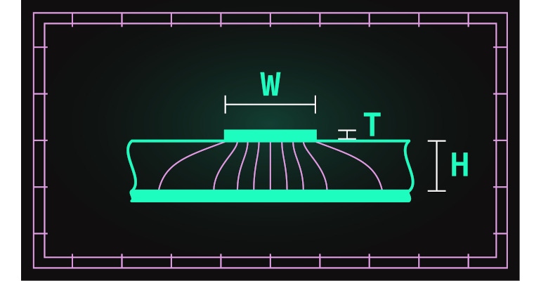
A designer is able to control the impedance of their traces by judiciously choosing the geometry of the trace and matching those dimensions to the substrate material properties. The major geometrical variables here are trace width, thickness, and distance to ground planes, all of which directly impact the impedance of a signal. Other material-based variables include substrate properties such as the dielectric constant. In practice, these values will be determined through the use of a PCB calculator that is often external to the PCB design tool.
Performing impedance matching will also vary based on the type of signal you have and how it's routed. For example, when working with differential signals, you must consider the coupling between signals in impedance calculations. Here, the distance between traces will also be an important variable in controlling the impedance. In many cases, high-speed signals will be routed as differential pairs.
5 Steps to Successful High-Speed Circuit Design
With a deeper understanding of high-speed circuit behavior and impedance matching, we’ll now explore some critical considerations for high-speed circuit design. The following 5 tips are things that I’ve learned over the course of my career as a hardware designer. If you implement these 5 considerations into your high-speed designs, you can rest assured that your circuit will perform as expected.
1. Match Impedances
As previously discussed, if you’re operating at high signal speeds, it is necessary to have controlled and matched impedances in your design. Your target impedance will be defined by the bus type you are working with (e.g., USB 90-ohm), and you must use the correct trace width and spacing to hit your target impedance and ensure that the impedance is consistent over the full path.
2. Use a Clean Ground (GND) Shield on Both Sides
High-speed signals are susceptible to noise and also create noise that impacts nearby signals. To minimize the effects of this noise in your circuit, it is wise to use ground (GND) shields on both sides of the signal. For example, if your signal is on PCB Layer 2, make sure that Layer 1 and Layer 3 surround the signal with a solid ground pour. Remember that your signal’s distance to GND is what defines its impedance, so don’t change the GND positioning without considering how it impacts impedance. Inconsistent ground references will also cause impedance discontinuities.
3. Use GND Vias at High-Speed Transitions
Generally, it is advised to avoid using vias when routing high-speed signals, but this isn’t always possible. When using vias is unavoidable, remember that as your signal pair changes layers, your ground reference must change layers as well. The signal’s characteristic impedance is defined by the signal and its return path. Hence, to keep impedance consistent and avoid reflections, you need to make sure that your GND return current has as clean a path as the signal itself. This means that if your signal pair is referenced to a given GND layer, and the signal pair is shifted to another layer, the original referenced GND layer must be shifted accordingly. Otherwise, return paths will be discontinuous and your characteristic impedance will be out of spec.
4. Length Matching
Beyond impedance matching, another important concept in high-speed circuit design is length matching. Signals have propagation delays that determine how long it takes for a signal to travel from transmitter to receiver. To ensure that signals arrive at the correct times, the length of the signal traces must be matched accordingly. A general rule of thumb is that a signal on a PCB will travel ~6 mil/picosecond.
Length matching can take two forms: P/N matching and bus matching.
P/N matching means you must ensure that the traces for both the P and N signals in a differential pair are matched to the same length. If they are not, the signals become susceptible to noise and radiation that negatively impact the signal’s bit-level reconstruction.
Bus matching means that, in signals that are referenced to a clock, the data signals must arrive at the receiver at the same time as the clock signal, or as close as possible. To do this, the bus signal traces must be equal in length to the clock signal.
5. Soften Impedance Discontinuities
A lesser-known tip is how to soften impedance discontinuities in a high-speed circuit. If you have an instance where your trace is not as wide as the pad it connects to, the point where the trace and the pad meet represents an impedance discontinuity (different widths = different impedances!) To soften this discontinuity, a trick of the trade is to void the GND plane underneath the pad (which has a larger width than the trace) and instead reference the pad to a GND plane one layer lower. By doing this, you will increase the distance between the pad and GND, and effectively offset the impact of the increased width on the impedance. This compensation will limit the impedance mismatches.
About the Author(s)
You May Also Like


