Tiny Image Sensor Targets the Metaverse
Backside illuminated shutter image sensor consumes low power and has tiny form factor for AR/VR and Metaverse products.

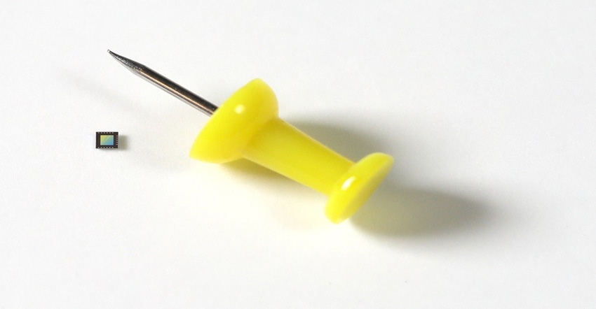
Metaverse and AR/VR applications are requiring sensors that not only provide high resolution but very small size. OmniVision Technologies has announced a three-layer stacked BSI global shutter (GS) image sensor for eye and face tracking in AR/VR/MR and Metaverse consumer devices, with a package size of just 1.64 mm x 1.64 mm.
The OG0TB sensor has a 2.2-µm pixel in a 1/14.46-inch optical format (OF). The CMOS image sensor features 400 x 400 resolution and consumes less than 7.2 mW at 30 frames per second. The combination of small size and low power consumption suits the sensor for tiny, battery-powered wearables such eye goggles and glasses.
The key to the sensor’s small size and processing capability is the use of a three-layer stacked design, which the company claims has not been utilized in image sensors. “Most mobile sensors today have two layers,” said Devang Patel, Marketing Director for IoT/Emerging segment at OmniVision, in a recent interview with DesignNews. “If you don’t move to stacking technology, you will not be able to shrink the pixel pitch much.”
In Omnivision’s GS sensor, two layers accommodate the pixel circuitry, with peripheral circuitry on the third layer. The three layers are wirebonded together. “The advantage of our architecture is that we can add more circuitry for intelligence and processing,” Patel added.
The sensor’s 1.64 mm square die size is currently the smallest in the industry, but Patel added that future sensors could see die sizes as small as 1.1 mm square.
The sensor’s Nyxel® technology enables high quantum efficiency (QE) at the 940nm NIR wavelength for sharp, accurate images of moving objects. The sensor’s high modulation transfer function (MTF) enables sharper images with greater contrast and more detail, which is especially important for enhancing decision-making processes in machine vision applications. Shutter efficiency is 106 dB.
The sensor supports a flexible interface, including MIPI with multi-drop, CPHY, SPI, etc.
The OG0TB GS image sensor is now available for sampling and will be in mass production the second half of 2023.
Spencer Chin is a Senior Editor for Design News covering the electronics beat. He has many years of experience covering developments in components, semiconductors, subsystems, power, and other facets of electronics from both a business/supply-chain and technology perspective. He can be reached at [email protected].
About the Author(s)
You May Also Like


.jpg?width=300&auto=webp&quality=80&disable=upscale)

