Semi Industry Pushing to Mainstream Chiplet Design
A recent wave of agreements and new platforms indicate progress in making chiplets a staple in packaging high-speed computing devices.

The performance and packaging advantages of chiplets have been fairly well documented, but there’s been a lag in creating some of the standards and development platforms needed to move the technology into more advanced stages of development. Some recent announcements hint that progress is being made, as the industry seeks to develop chip packaging solutions for new generation of high-speed computing solutions for applications such as artificial intelligence (AI).
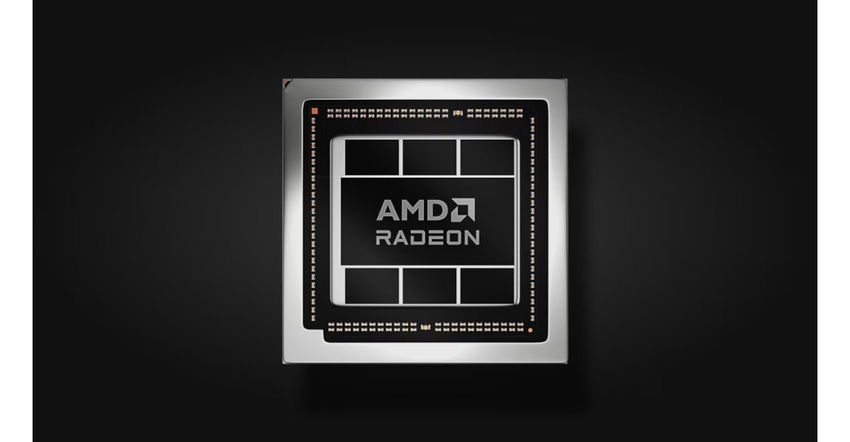
Top-tier semiconductor companies such as Intel, AMD, and Nvidia have been trying to top another by incorporating chiplet designs in some of their latest chips. AMD has fired the latest salvo, unveiling its 7900M laptop graphics processor, reportedly the company’s first with a chiplet design. The GPU features AI accelerators and second-generation ray-tracing accelerators.
One key advantage of chiplets is the potential to reduce the time to market developing custom parts. Zero ASIC, a semiconductor startup, is now offering early access to its ChipMaker platform. The chiplet platform enables users to design custom ASICs without coding, as well as providing interactive RTL-based chip emulation.
By masking the complexities of circuit design inside a reusable validated chiplet, Zero ASIC is aiming to help user both cut the costs and reduce the lengthy time-to-market developing a custom ASIC. The platform enables automated design, validation, and assembly of System-in-Packages from a catalog of known good chiplets. Users can test out their custom designs quickly and accurately before ordering physical devices, using cloud-based FPGAs to implement the RTL source code of each chiplet in a custom SoC.
Standards Activity
One key to promoting adoption of chiplets is developing standards that would eventually create a mass market for chiplet parts. Recently, the Open Compute Project Foundation (OCP) and JEDEC announced they would merge the capabilities and open standards of OCP’s Chiplet Data Extensible Markup Language (CDXML) and JEDEC’s JEP30 PartModel Guidelines. This partnership, initiated in late 2022, promises to revolutionize chiplet design, manufacturing and integration. The result will be a unified structure that supports both chiplets and general electronic parts within the JEDEC.
Integrating the OCP CDXML into JEP30 will enable chiplet builders to provide standardized chiplet part descriptions to their customers electronically. Proponents believe this will open the door to automate System in Package (SiP) design and assembly using chiplets. The chiplet descriptions encompass crucial information for SiP builders, including thermal properties, physical and mechanical requirements, behavior specifications, power and signal integrity properties, testing in-package and security parameters.
Meanwhile, the UCIe (Universal Chiplet Interconnect Express) consortium, a group developed several years ago, recently updated its specifications to extend reliability mechanisms to more protocols and support broader usage models. Additional enhancements are included for automotive usages – such as predictive failure analysis and health monitoring – and enabling lower-cost packaging implementations. The specification also details architectural specification attributes to define system setups and registers that will be used in test plans and compliance testing to ensure device interoperability.
On the production end, more chip IP companies are teaming with semiconductor foundries to bring chiplets to market. Earlier this month, Tenstorrent, a company that sells AI processors and licenses AI and RISC-V IP, announced it has selected Samsung Foundry to bring Tenstorrent's next generation of AI chiplets to market.
Tenstorrent builds RISC-V CPU and AI acceleration chiplets, aiming to push the boundaries of compute in multiple industries such as data center, automotive and robotics. These chiplets are designed to deliver scalable power from milliwatts to megawatts, catering to a wide range of applications from edge devices to data centers. The chiplets will be manufactured using Samsung's state-of-the-art SF4X process, which boasts an impressive 4nm architecture.
Recently, Faraday Technology Corp., an ASIC design service and IP provider, launched its 2.5D/3D advanced package service. The company will leverage its interposer manufacturing service for chiplets connection and close collaboration with top-tier foundry and OSAT suppliers to secure capacity, yield, quality, reliability, and schedule in production.
Faraday enhances flexibility and efficiency in advanced package service for multi-source chiplets, packaging, and manufacturing. In a long-term partnership with leading semiconductor foundry UMC and premier OSAT vendors in Taiwan, the company can support custom custom passive/active interposer manufacturing, and proficiently managing 2.5D/3D package logistics.
About the Author(s)
You May Also Like


