Thin Light-Emitting Device Advances Design of Invisible Displays
Researchers at UC Berkeley have developed a bright-light emitting device that is so atomically thin that it’s fully transparent when turned off.
May 1, 2018

Screens that virtually disappear when turned off are the future of display technology. Researchers at UC Berkeley are a step closer to achieving this goal with the invention of a bright-light-emitting device that is so atomically thin that it’s fully transparent when turned off.
The researchers in UC Berkeley’s Department of Electrical Engineering and Computer Sciences used a monolayer semiconductor just three atoms thick to develop the device, said Der-Hsien Lien, a postdoctoral fellow who worked on the project. The lab of Ali Javey, professor of electrical engineering and computer sciences, produced the device.
Its invention paves the way for invisible displays on walls and windows that would be bright when turned on but transparent when turned off, researchers said. It even could lead to next-generation technology, such as light-emitting tattoos. It’s the thinness of the semiconductor that allows for the display’s invisible appearance by the way it interacts—or rather, doesn’t interact—with other materials, Lien stated.
|
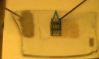
Probes inject positive and negative charges in a light-emitting device invented by researchers at UC Berkeley. The device is transparent under the campanile outline, producing bright light. (Image source: Javey Lab, UC Berkeley) |
“For this thickness, a majority of visible light—wavelengths ranging from 400 to 700 nanometers—penetrates the material without too much interaction with the materials. So the absorption is low [or about] 10 percent, which means 90 percent of light penetrates the material,” he explained. “When the device is off, no light is emitted from the monolayer, so you can see through the material and see the background.”
Researchers also switched certain materials in the device from opaque to transparent to achieve the disappearing effect—specifically, silicon and nickel for quartz and indium tin oxide, respectively, Lien said.
Commercial LEDs function using a semiconductor material that is electrically injected with positive and negative charges. These charges produce light when they meet. Typically, these types of devices use two contact points: one for injecting negatively charged particles and one for injecting positively charged particles. Making contacts that can efficiently inject these charges is a persistent challenge for designers of LED technology—particularly in monolayer semiconductors with limited material.
The Berkeley team solved this challenge by designing a new device that only requires one contact on the semiconductor. Laying the semiconductor monolayer on an insulator and placing electrodes on the monolayer and underneath the insulator allowed the researchers to apply an AC signal across the latter, they said.
READ RELATED ARTICLES HERE:
The device creates light through the presence of both positive and negative charges during the moment when the AC signal switches its polarity from positive to negative, and vice versa, according to the researchers. The team showed that this mechanism works in four different monolayer materials—all of which emit different colors of light.
Researchers published a paper on their work, which was funded by the National Science Foundation and the Department of Energy, in the journal Nature Communications.
Design Strengths And Flaws
The design of the device has a number of advantages, Lien told Design News. From the aspect of developing a display, one is that the size of the device is highly scalable, he said.
“A device, as a pixel, can be made in the range of micrometer, so the resolution of the display can be high,” Lien stated. “The size of the device/screen can also be large. The largest device we show in the study is in the range of millimeter scale. So far, we are limited by the size of the monolayer film we can grow. In principle, the size of the screen is unlimited.”
The device still has limitations, however. Researchers plan to continue their work particularly to improve its efficiency, which is only around 1 percent, they said. In comparison, commercial LEDs have efficiencies of about 25 to 30 percent.
Elizabeth Montalbano is a freelance writer who has written about technology and culture for 20 years. She has lived and worked as a professional journalist in Phoenix, San Francisco, and New York City. In her free time, she enjoys surfing, traveling, music, yoga, and cooking. She currently resides in a village on the southwest coast of Portugal.
About the Author(s)
You May Also Like


