Specifying & Creating Data-Acquisition Systems, Part 2
March 6, 2012

Our February column, the first in a series on specifying and creating data-acquisition systems, emphasized analog-to-digital-converter (ADC) resolution and accuracy.
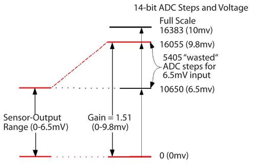
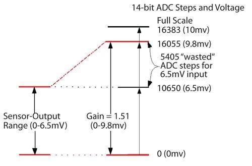
The ADC modules and boards used for data acquisition (DAQ) offer bipolar input ranges of plus or minus x volts, or unipolar ranges of 0-y volts. Just as digital voltmeters have several input ranges, so do ADC modules. But rarely do the sensor voltages completely "fill" these ranges. A 6.5mV sensor output, for example, connected to a 0-10mV ADC input leaves 35 percent of the range unused, as shown in the figure below. For simplicity's sake, I'll assume an ideal 14-bit successive-approximation ADC (214 = 16384), so the LSB has a step size of 10 x 10-3 V / 16383 steps, or 0.610 V.

An amplifier placed before the ADC input could boost the 6.5mV sensor output to a maximum of, say, 9.8mV, which comes close to full scale without exceeding it. By "spreading" the 6.5mV signal across a greater span of 16383 ADC steps, you increase the apparent resolution. A 9.8mV signal would represent 16055 steps for the ADC, so for the original sensor signal you now have:
6.5 x 10⁻³ V / 16055 steps or 0.405 V/steps
The ADC steps remain 0.610V, but each step represents 0.405V from the sensor. You can use the scaling ratio, 1.51 (9.8/6.5), later to calculate actual sensor voltages.
A home-brew amplifier circuit with a gain of 1.51 would boost the 6.5mV signal to 9.8mV, but commercial programmable-gain or instrumentation amplifiers do the job better. Programmable-gain amplifiers offer fixed-gain values, usually in steps of 1, 2, 4, 8 .., 1, 2, 5, 10 .., or 1, 10, 100 ... But none equals 1.51.
About the Author(s)
You May Also Like


