How Chip Technology Can Help Diagnostics Manufacturers
An industry expert explains how chip technology can contribute to cost-aware efficiency gains in diagnostics devices as well as open up new application markets.
September 2, 2020
Olivier Henry of Imec
In times where the entire healthcare sector is going through fundamental transitions, diagnostics providers face competitive challenges and margin pressures. To establish and maintain a competitive position in this growing market, the willingness to adopt state-of-the-art technologies and innovations might prove to be key. Here's how chip technology can contribute to cost-aware efficiency gains in diagnostics devices as well as open up new application markets.
Diagnostics manufacturing is facing considerable challenges and opportunities, driven by an entire healthcare sector that is moving toward more personalized and patient-centric business models and value propositions. As a consequence, there is for example an increased demand by physicians for companion diagnostics: tests that predict the likelihood of a given treatment being suitable for a specific patient and that can monitor the therapeutic effect during the treatment. Leveraging on these and other trends, the Global IVD Market Report predicts the in-vitro diagnostics market (IVD) will show a cumulated average growth rate (CAGR) of 6,6% from 2018 onward and reach almost $100 billion in 2023.
To successfully tap into this market, competitive firms need to relate the latest and greatest in technology, which is fuelling the personalization wave and has a high impact on the healthcare sector. Yet, while the tech giants and start-ups are moving into healthcare, a rather reluctant attitude can still be observed from within the established diagnostics suppliers. A reservation that might partly result from a lack of knowledge about the chip technologies that are out there, ready to be implemented.
High quality at low cost
Whether it is a pregnancy, lactate or glucose test, or any other diagnostic support for consumer healthcare, the most widely used materials to capture and manipulate samples are paper and plastics. And for an obvious reason – cost – in a lot of cases these materials will remain the best candidate for the foreseeable future.
Yet increasingly, contexts emerge where there is a demand for higher accuracies or added functionality. For example, in fast diagnostic tests that require sequencing, or that do not allow for substrate-dependent (strip-to-strip) variations. If you need a low-cost and convenient diagnostics device that can give you similar results as the ones obtained in laboratory conditions, silicon and related semiconductor technologies are your best option. Backed by a mature ecosystem, almost any complex chip can be mass-manufactured in higher volumes at an acceptable price level for high-value diagnostics applications.
Chip technology: a toolbox of versatile building blocks
Part of what makes semiconductor technologies’ strength is the diversity of highly miniaturized components that can be built into and onto a chip. Extremely precise manufacturing processes allow to build channels and structures to perform complex microfluidic handling steps very easily: move samples from A to B, generate droplets, encapsulate targeted objects, merge them or filter them out, concentrate or dilute them, etc.
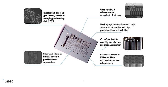
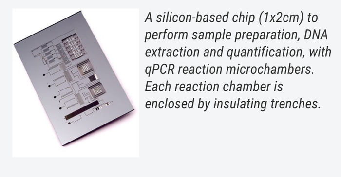
Overview of some of the micro- and nano-electronic structures that can be integrated into a silicon lab-on-a-chip. Center: a silicon-based lab-on-a-chip (1x2cm) to perform sample preparation, DNA extraction and quantification, with qPCR reaction microchambers. Each reaction chamber is enclosed by insulating trenches.
Another one worth highlighting is photonics: a well-known technology used in, for example, glass fibres to transport data in a more efficient way. But photonic waveguides and other components can also be used for applications in life sciences. Photonics-based solutions offer high-sensing performance in combination with compact system integration. They are robust as they do not need optical alignment or calibration steps. And photonics is compliant with the demand for low-power consumption and low-production cost. Developed by universities, start-ups, and research institutes, a full library of photonic components is available for companies to build the next generation of photonic biochips.
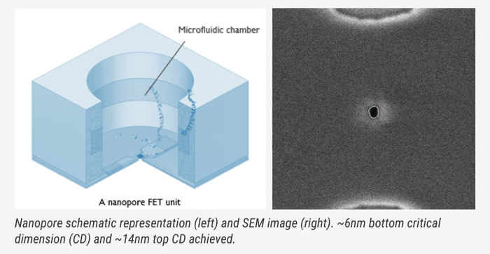
And there is more. For example, nanopores: nanometre-wide structures on chip, which help allow for a large-scale integration and measurement bandwidth. This large bandwidth can allow other type of investigations as well, going toward, for example, direct protein identification based on their rotational/diffusion properties in the pore, in a label-free fashion.
In brief: silicon chips enable rapid sample-to-diagnostic workflows and are ready to revolutionize diagnostics, just as they did with our smartphones.
Devices and applications
The examples below illustrate the capabilities of these silicon technologies for a multitude of applications: measuring physical, chemical, and biochemical parameters. By customizing these technologies, it is a small step to further advance fast, reliable, and cost-efficient diagnostics devices.
On-chip molecular biology
Looking at the typical DNA sample preparation and workflow, today there are many challenges: the multitude of manual steps in a complex workflow, the low diagnostic accuracy and irreproducibility of results and the high cost per genome (reagents cost over $200 per sample prep). Imagine all lab functionalities needed for sample-to-result being shrunk and placed on a chip and enabling full PCR analysis from whole blood in less than 10 minutes.
Imec developed such a silicon lab-on-a-chip that can perform sample preparation, DNA extraction, and quantification, and that includes small reaction chambers to carry out a fast and full PCR reaction. The PCR cavities consist of a microreactor, integrated aluminum heaters, thermal insulation trenches and microfluidic channels to complete a standard DNA amplification within five minutes. As such, a full laboratory workflow can be integrated on a single silicon lab-on-a-chip.
Thanks to its extreme miniaturization and parallelism (i.e. capability of processing multiple samples at once), chips like these could be of high value for diagnostics. An imec study by Cai et al. - in collaboration with three Flemish universities and published in Clinical Chemistry 2018 - demonstrates sensitive and qualitative on-chip detection of group B streptococcal infection in pregnant women samples in under five minutes. It is just one of many possible applications of this type of chip technology to the rapid and sensitive detection of viruses and bacteria in clinical samples.
Integrated (bio)chemical sensors driving lab-on-a-chip systems
By analysing by-products of cell metabolism – proteins and enzymes – either being taken up from or secreted into the culture medium, the biological state of cells can be determined. Current technologies, for example, based on immunoassays, mass spectrometry, chromatography, or spectroscopy are not always available in on-line setups, require large efforts in sample preparation, and often lack specificity in complex culture media with a high protein background.
The mainstream approach for protein detection and quantification is the use of immunoassays (i.e. ELISA). In one of its many variants, detection antibodies – labelled with enzymes of fluorophores – are used to increase the sensitivity and specificity. A drawback is that any unbound labels need to be washed away before the measurement can be performed, complicating the overall workflow and increasing the time to result. As an alternative, many label-free techniques have been explored, but these invariably suffer from poor specificity and, hence, have poor limits of detection in complex matrices.
As an alternative, one could turn to photonic-based immunoassays. For example, with the use of photonic waveguides, Imec has built a fluorescent immunoassay which could be used to monitor relevant proteins in medical diagnostics. Its specificity, sensitivity, and detection limits are comparable to ELISA, but it allows a rapid kinetic, wash-free read-out. The key element of this immunoassay is a photonic chip, which could be easily integrated in a point-of-care diagnostics. It is a generic technique and any protein of interest can be detected with this immunoassay platform.
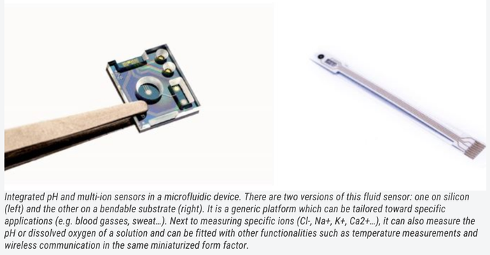
A similar story as for photonics-based biosensors can be told for ion sensing and fluid monitoring, for example, for measurements of blood gasses or to analyse sweat. Typically, these involve large expensive sensors that are dedicated to one (or very few) target ions. Thanks to chip integration, it is possible to make similar systems with comparable (or even better) performance metrics on a surface area of only a few square centimeters.
Imaging, spectroscopy, and cell sorting
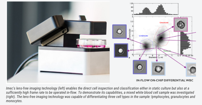
For some diagnostics (e.g. in cell therapy and its bioprocessing) it is important to have a visual inspection of the cells’ morphology to get direct feedback on the viability and overall condition of the cells. Normally this is performed by a process operator who takes a sample for inspection with a microscope. This manual observation holds significant limitations, as certain characteristics are almost impossible to correctly quantify. Also, this evaluation typically suffers from operator-to-operator variability.
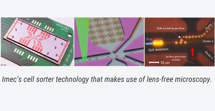
Thanks to lens-free imaging cytometer technology this inspection can now be automated and integrated. Such lens-free system uses a coherent light source (e.g. LED or laser) and a CMOS imager to capture the light that is diffracted off small objects such as cells. Custom software algorithms reconstruct the captured diffraction pattern (called hologram) into an in-focus image that resembles the cell that is being imaged. It is a compact solution, which enables a large field of view and very good resolution, at an affordable price. Machine-learning-based image analyses and powerful classification algorithms can assist to evaluate the images and differentiate between specific cell types.
Aside from visual imaging, for a lot of contexts (e.g. to identify materials – fluids, powders, solids) spectroscopic imaging solutions, such as Raman spectroscopy, come into play. Literature already reports on the potential of Raman spectroscopy for medical diagnostics, ranging from in-vitro biofluid assays to in-vivo cancer detection (Kong et al., Advanced Drug Delivery Reviews, 2015).
Raman functions by shining laser light on the material and creating a spectral chart from the analysis of a specific part of the scattered light. In this chart, one can recognize the spectral ‘fingerprint’ of each material and compound. A well-known spectrometer is based on the Michelson interferometer. The disadvantage of this design – particularly if you want to miniaturize it – is that two mirrors are used, one of which moves. Thanks to a different fundamental approach, it is possible to build an integrated photonics version of such a scheme. One without moving parts. Such miniaturized Raman spectrometer is better fitted to comply with the requirements for smaller and more convenient diagnostics tools.

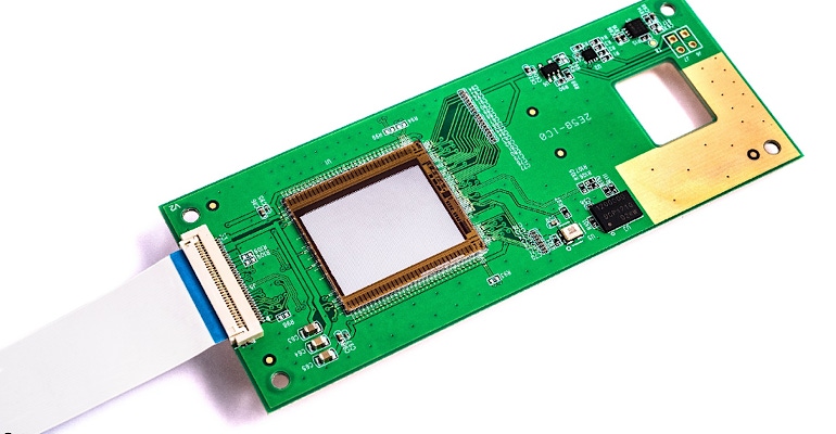
Imec’s on-chip Raman spectroscopy solution, using a million interferometers on top of a CMOS image sensor. This build-up allows for extreme miniaturization and, using chip technology, the price of the device can be much lower than current devices.
However, before cells can be monitored or manipulated, various lab-on-chip solutions require sorting and isolation of cells. Miniaturized cell-sorting mechanisms can be seen as a key enabler for a variety of the devices already described. Such cell-sorter chips are currently under development and rely amongst others on label-free identification, micro-acoustics and microfluidic jet-flow techniques to recognize and sort cell types from complex biological samples, as for example, peripheral blood mononuclear cells (PBMC).
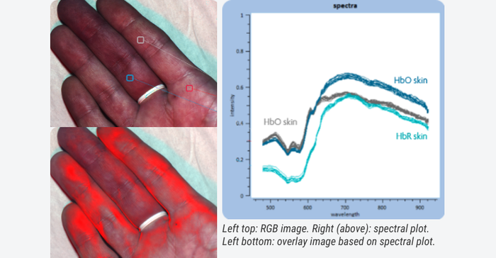
Combining the best of both worlds, imaging and spectroscopy, there is the domain of hyperspectral imaging. Tuneable to almost any given wavelength, and combinations thereof, a myriad of solutions are already commercially available with which extra dimensions can be created to what can be seen with the naked eye. Think of obtaining real-time visual feedback on blood oxygenation during surgery, skin diagnostics, wound care management.
Point-of-care diagnostics and future avenues
All of the technologies above support the gradual but irreversible trend toward diagnostics that are closer to the point of care. From the multitude of options in research and development, a variety of spin-offs and start-ups have already emerged. In growing numbers, they lead the way into bringing miniaturized, rapid, easy-to-use, lab-quality tests with built in connectivity directly to the patient and clinician.
Lots can also be expected from future avenues such as ingestibles (electronic devices that can be swallowed and have the capability to sense and actuate inside our digestive tract), and implantables. With neuroprobes (miniaturized probes for mapping and in a later stage also stimulating brain activity) as maybe amongst the ones that trigger most imagination. Clearly sufficient foundation to claim that silicon technologies can revolutionize the diagnostics and related industries.
About the author
Olivier Henry, PhD, is the program manager for life science and medical device technologies at Imec. His research interests and expertise lie in the development of new integrated microdevices with application in diagnostics, chemical and biochemical synthesis, and cell and tissue microengineering. He has co-authored more than 40 peer-reviewed publications and holds several patents in the field of polymer and electrochemistry, microfluidics, sensing, and diagnostics.
You May Also Like
