Fast Forward to a New Generation of Miniature, Wireless, High-Density Brain Implants
A new low-power, miniature chip 16 times smaller than the state of the art coupled with advances in wireless data transmission and sensing could enable the next leap in miniature wireless brain implants.
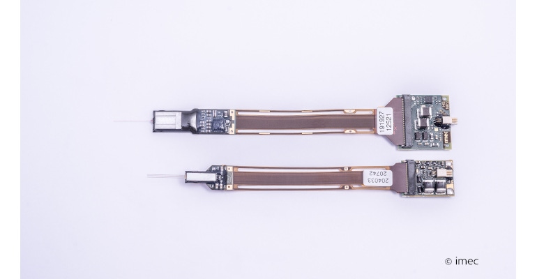
Brain implants are tiny devices covered in electrodes or sensors to stimulate or record brain activity from neuron cells. Surgeons implant them to restore a lost function (think about cochlear implants for hearing loss) or to help patients with, for example, Parkinson’s, depression, and epilepsy when medication fails. Research into implants focuses on making the devices smaller, driving up the number of electrodes while maintaining low power consumption. Smaller devices are less invasive and limit scar tissue buildup, which in turn ensures long-term performance since neuron activity is often attenuated by healing tissue. An increased number of electrodes provides more fine-grained electrical recording and stimulation for more-precise therapy or research. And, as the implant becomes more intricate and size decreases, ultra-low power circuits will be a must.
Imec’s Neuropixels implants are currently state of the art in research and have recently been implanted in the first humans to receive such devices. More than 900 labs worldwide use these neural probes. The first version had 1,000 electrodes, which more than doubled in Neuropixels 2.0 with over 5,000 electrodes on four 70-by-24 µm2 implantable shanks attached to a 2.2 × 8.7 mm2 base chip. (See image above.) Meanwhile, imec is already looking beyond the horizon to the future probes that are even smaller while keeping a high electrode count. Carolina Mora Lopez, scientific director and team leader of the Circuits for Neural Interfaces Team at imec, and her team designed a new miniature prototype chip for recording brain signals. It’s 16 times smaller than the first Neuropixels generation.
Downsizing the Neural Probe’s Real Estate
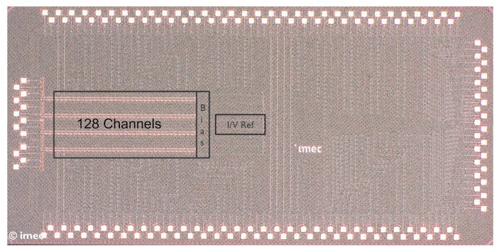
Such miniaturization (total area per channel of 0.005 mm2) was achieved by applying smart design solutions on the one hand and harnessing the advantages of a smaller technology node on the other hand.
The team reduced the number of circuits while still realizing the same functionality and performance in terms of metrics such as noise (7.7±0.4 μVrms in the AP band and 11.9±1.1 μVrms in the LFP band) and power consumption (total per channel of 8.34 μW) by using circuit techniques based on a ‘direct digitization’ architecture. Direct digitization aims at converting the weak neural signals from the analog to the digital domain as close as possible to the electrodes that capture them. This approach saves area by reducing the number of amplifiers and filters. Moreover, it improves the signal quality as analog signals do not need to travel long distances.
However, existing direct digitization front ends still consume high power, exhibit a limited bandwidth to tolerate movement/stimulation artifacts, or feature a limited electrode DC offset cancellation. DC offset is a constant baseline voltage that exists without a neural signal. These voltages are problematic because they superimpose on the brain signal and can saturate the recording channel. The new chip tackles these challenges using a combination of a Δ-ΔΣ modulator with an AC-coupled input stage. The Δ-ΔΣ modulator digitizes the analog signals with an increased dynamic range three times higher than the most advanced Neuropixels probe available (43 mVpp), while the capacitor provides rail-to-rail electrode DC offset cancellation (i.e., both for the lowest and highest possible voltage levels). Having AC coupling in front of the Δ-ΔΣ modulator further reduces the power consumption since only AC signals are digitized.
Tapping into Smaller Technology Nodes
The push toward thousands of electrodes urged the engineers to look at smaller nodes to keep the area of the probe as small as possible. With this new prototype, the team explored for the first time a 22-nm CMOS technology. This is previously uncharted territory for brain implants because technologies below 130-nm technology (what is used in Neuropixels) employ copper metallization, which is potentially harmful to brain cells. Therefore, one of the aims of the new chip design is to explore copper toxicity in depth and come up with solutions if it presents an issue.
Even though the new prototype holds fewer recording channels than Neuropixels (128 versus 384), it achieves one of the smallest areas and lowest power per channel while providing electrode DC offset cancellation over the entire voltage range, good noise performance, and improved bandwidth. Furthermore, this direct-digitization approach is highly scalable to hundreds of channels. It thus holds the promise of even higher-density neural probes than already exist today.
Cutting the Wires
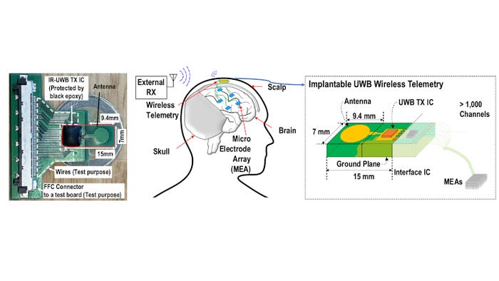
We want to make the whole probe system fully implantable: a must for future clinical implementation and chronic implantation. Head-mounted telemetry modules have already been miniaturized and implanted below the scalp for transcutaneous data transmission. By distributing multiple high-density probes, such as Neuropixels, across the brain, neuroscientists have begun to map the correlation of neuronal activity across different brain regions. However, multiple high-density probes create an enormous amount of data. There is currently no wireless technology that can transfer these gigabytes of information through the skin to an external readout. State-of-the-art devices are typically built for less than 100 channels of wireless capacity, while multiple Neuropixels require a wireless interface to support a few thousand. Not only is the data rate important, but also are size and power consumption. A smaller device requires less invasive surgery, while low power avoids tissue damage from heating. Yao-Hong Liu, scientific director at imec, and his team are focused on creating such an energy-efficient, miniaturized, and high-bandwidth wireless interface that is up for the challenge.
Ultra-Wideband Technology for Gbps Transcutaneous Data Transmission
Ultra-wideband (UWB) technology shows promise for wireless interfaces for brain implants because of its ability to transmit data at high speeds while consuming minimal power. The team pushed the envelope even further to support an incredible 1.66 Gbps of data communication over a 2-cm distance. Even though that is already two times the transmission range of most implantable UWB radios, we need to cover even longer distances. With wireless communication from the probe to an outside device in mind, a transmission range of up to 10 cm is recommended to improve the reliability of the wireless link against, for example, antenna misalignment. Imec solved that by proposing an innovative modulation scheme called hybrid impulse modulation. While traditional UWB systems typically employ pulse-based modulation schemes, the hybrid approach combines impulse-based modulation with continuous wave components. The hybridization of the signal improves the robustness of the communication, maintaining signal integrity when transmitting through biological tissue. The resulting telemetry system enhances the communication distance from 2 cm up to 15 cm while at the same time maintaining a high data rate of 1.43 Gbps without increasing the overall power (energy consumption of 5.8 pJ per bit). This is at least 16 times better than the state of the art.
Toward Free-Floating Neural Probes
Meanwhile, the team is working on cutting even more cables. Current implants still have a direct cable connection between the probe and the head-mounted or subcutaneous module. Because the brain moves like jelly and the probe is rigid, the strain from these wires can cause scars in the tissue around the probe, which can completely corrupt recording signal quality in a few years or even months. The obvious solution is completely removing the cables between the skull and the probe. That means you can cover the dura (the membrane under the skull protecting the brain) entirely and make the probe free-floating so it will move in pace with the brain and not cause scar tissue.
Less obvious is how to implement the solution. Such a device must be small enough to fit under the skull. With the advances in surgery, new burr-hole or twist-drill craniotomies safely expose a small area of the brain (less than 10 mm) for probe implantation, allowing the skull to heal faster than traditional large-area craniotomies.
However, the existing wireless telemetry solutions are still too large for implantation under the skull. At these millimeter scales, we cannot use conventional radio approaches. Inductive coupling is widely adopted in implantable devices for wireless power and data transfer but does not offer sufficient bandwidth. Optical communication has been demonstrated to have adequate bandwidth for data transmission and has a small footprint, but the propagation distance is limited given the scattering nature of the dura and brain fluid.
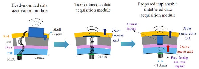
The imec team thus resorted to body channel communication (BCC). Instead of traditional wireless methods like radio waves or electromagnetic fields, BCC relies on the conductivity of the human body to transmit signals. Galvanic-coupled BCC are commonly used for on-body to on-body or to implant communication with skin-attached electrodes. Implant-to-implant applications exist but not at the high bandwidth needed for this application. Imec now demonstrates a transdural link (between the brain and the skull) based on galvanic-coupled BCC. It features a miniature implantable transmitter to transfer the neuroprobe’s data at an incredible >250 Mbps data rate over the dura to a receiver in the burr hole. Moreover, this system tolerates a horizontal misalignment up to ±4 mm, corresponding to the brain's reported relative motion range.
Processing Neural Data Like the Retina and the Brain
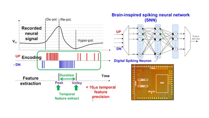
Parallel with the efforts to build a wireless interface that can support a high data rate, Yao-Hong Liu’s team also explores ways to compress the data. To design their new neuromorphic sensing system (NSS), they turned to our own neurons for inspiration. Look, for example, at the human retina. Our eyes pick up a massive amount of (often very complicated) information passed via the retina to the back of our brain using very little energy. Interestingly, the brain has no problem reconstructing these images at high resolution. What happens is that the neurons in the retina will only react when they notice changes, not when the information is static—a phenomenon called delta modulation. In doing so, it is possible to compress the data a hundredfold. The resulting bio-inspired NSS demonstrated a data compression ratio of >125 times while maintaining the data fidelity (normalized RMS error of 4 percent) and, at the same time, barely requiring energy. Furthermore, by mimicking our visual cortex using edge computing based on spiking neural networks, the NSS can extract temporal signatures of the recorded neural signal (e.g., peaks or valleys) with a precision and latency down to 10 µs. This enables continuous monitoring with extremely low power consumption (28 mW) and real-time adaption of neural stimulation for therapeutic purposes.
Looking Beyond the Horizon
By improving on multiple fronts—the neural probe, the wireless data transmission, and the data itself—imec aims to create the next generation of large-scale, high-quality wireless implants. The challenge will now be to validate all puzzle pieces further and bring them together in one system.
Want to Know More?
Carolina Mora Lopez’s team works on the direct-digitization readout was presented at the 2022 IEEE VLSI Symposium on Technology and Circuits [https://www.imec-int.com/en/press/imecs-new-direct-digitization-readout-design-enables-small-low-noise-low-power-neural] and received an Honorable Mention at the Brain Best-Paper Award for her conference paper, Yang et al., "A 128-Channel AC-Coupled 1st-order Δ-ΔΣ IC for Neural Signal Acquisition." 2022 IEEE Symposium on VLSI Technology and Circuits (VLSI Technology and Circuits), Honolulu, HI, USA, 2022, pp. 60-61.
Yao-Hong Liu’s team presented the low-power ultra-wideband transmitter chip at the 2022 International Solid-State Circuits Conference (ISSCC) [https://www.imec-int.com/en/press/imec-pioneers-ultra-wideband-transmitter-chip-pushes-data-rates-166gbs-milliwatt-power] and received an Honorable Mention at the Brain Best-Paper Award for his conference paper, Song et al., "A 1.66Gb/s and 5.8pJ/b Transcutaneous IR-UWB Telemetry System with Hybrid Impulse Modulation for Intracortical Brain-Computer Interfaces." 2022 IEEE International Solid-State Circuits Conference (ISSCC), San Francisco, CA, USA, 2022, pp. 394-396.
The work on the transdural link has been published in Shi et al., "Galvanic-Coupled Trans-Dural Data Transfer for High-Bandwidth Intracortical Neural Sensing." IEEE Transactions on Microwave Theory and Techniques, vol. 70, no. 10, pp. 4579-4589, Oct. 2022.
The project “Intranet of Neurons” (IoN) on the transdural link and data compression has received funding [https://www.imec-int.com/en/press/prestigious-erc-consolidator-grant-awarded-imecs-yao-hong-liu-develop-miniature-energy] from the European Research Council (ERC) under the European Union’s Horizon 2020 research and innovation program (grant agreement No.101001448). Recently, Yao-Hong Liu received a complementary ERC 2023 Proof of Concept grant program, SpikeZip (grant agreement No. 101138283), to support the proof-of-concept development extended to biological validation.
You can read more information about Neuropixels in a previously published article [https://www.imec-int.com/en/articles/eavesdropping-brain-10000-electrodes] and press release [https://www.imec-int.com/en/press/latest-neuropixels-probes-can-track-neurons-over-weeks].
About the Author(s)
You May Also Like


