Sensors Bring Silicon Closer to System
Semiconductor chip tool vendors now face life-cycle issues in embedded IoT sensor designs that require serious silicon lifecycle management.
December 2, 2020

Anytime one of the big three electronic design automation (EDA) chip tool vendors talks about system-level or life-cycle development, it’s time to listen. Of course, each of the big three giants– Synopsys, Mentor-Siemens, and Cadence – have their own inflection, their own interpretation, and focus, in the larger system electronics world. For Synopsys, that focus has been on the interface (e.g., USB) verification intellectual property (P) space, software at the chip and embedded board levels, and chip reliability. Their most recent announcement reflects the latter focus with its life cycle awareness of certain types of sensor chips – from design through operation and maintenance.
It also reflects a bigger effort in the semiconductor chip industry to move into the larger systems community. This is a natural trend as chips – to some measure – have become commodity items, a critical element but just part of the larger embedded, package, and system space.
Still, the basic design and verification of highly complex hardware systems-on-chips (SoCs) have not gotten easier. The complexity has been further increased with security issues, the growing role of end-user software developers, production yield problems during manufacturing, reliability challenges at smaller node geometries, and more. What is needed is a way to view and optimize the entire lifecycle development of SoCs, from the design phase through end-user deployment, manufacturing, operation, and even maintenance.
One such lifecycle platform has been announced by Synopsys, an Electronic Design Automation (EDA) vendor. The company stated that its Silicon Lifecycle Management (SLM) platform will provide visibility into critical performance, reliability, and security issues for the entirety of a chip's lifespan. It will also provide something fairly new at the system-level, namely, post-silicon analysis, maintenance, and optimization.
To enable this system perspective requires that the platform gather as much useful data about each chip as possible and analyze that data throughout its entire lifecycle. Gathering this data has been made easier with Synopsys’s recent acquisition of Moortec, a provider of in-chip monitoring technology specializing in process, voltage, and temperature (PVT) sensors. Taken as a whole, the company’s new lifecycle platform should provide actionable insights into improving chip and system-related (i.e., software) activities.
To learn more about this life-cycle approach to chip design, Design News reached out to Steve Pateras, Ph.D. in EE and Senior Director of Marketing, Hardware Analytics and Test at Synopsys. What follows is a portion of his insights.
DN: Concerning the Silicon Lifecycle Management Platform: These types of platforms are commonplace in the world of larger system-of-systems (SoSs) engineering. What makes Synopsys’s entry unique?
Steve Pateras: Product lifecycle management has indeed been around for a while for systems as a whole. Our application of this concept to silicon devices is new and a critical component to addressing system-wide lifecycle management. Optimizing electronic systems requires visibility and optimization at the device level. Specific unique platform features:
Monitor data and targeted data analytics that directly drives design optimization
Monitor data and targeted data analytics that directly drive yield ramp and optimization
Monitor data, targeted data analytics, and direct ATE control for test optimization
These unique ties into the design as well as manufacturing and test also enable unique insights and optimizations at the later bring-up and in-field stages of the lifecycle. Indeed, the platform’s span of the entire lifecycle allows for unique traceability related optimizations. For example, obtaining and analyzing baseline design performance metrics allows for tracking and predicting performance trends once the product is in the field.
DN: How have engineers dealt with the lifecycle management of the chip development process in the past?
Steve Pateras: There have been various ad-hoc and proprietary approaches to managing some aspects of the silicon lifecycle but nothing commercial or comprehensive in nature. For example, some large chip vendors have developed proprietary in-chip sensors but the use of these sensors and sensor data has been limited in scope. Very little if any analytics have been used on the data and the sensors have been used for only a limited part of the lifecycle (silicon bring-up for example but not for yield improvement or in-field optimization)
DN: There is plenty of global tension in the semi supply chain. Does this tool take these kinds of potential design-supply constraints into account?
Steve Pateras: The data generated by the monitors and sensors is owned by whichever customers generate it. For example, chip vendors own data generated during the test or bring up phases. System integrators will own data generated by the monitors and sensors generated while operating in the system. Each customer can then make use of the analytics engines to process their own data. Having said this, there will be value in sharing data across the supply chain as well. System integrators or operators could for example use data generated early on in the lifecycle as a baseline to understanding trends during in-field operation. Since the sharing of data in both directions will be useful to all players we are hopeful that they will be open to sharing at least some aspects of their data.
DN: Why is it necessary to provide, “access to device data throughout the entire chip life span?”
Steve Pateras: Data obtained from the chip at each lifecycle stage can provide insight into how to optimize that stage. For example, data obtained during tests can help to improve test efficiency and test quality while data obtained during system bring-up can help to improve time-to-market through a faster uncovering of any functional issues. Data accumulated over the entire lifecycle can also provide additional insight at individual lifecycle stages. For example, tracking performance metrics like path delays from initial bring-up to in-field operation can help improve timing models that can be used in subsequent designs for improved margins.
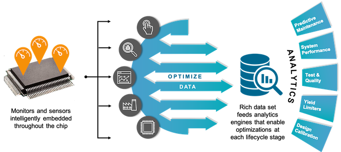
Through the use of monitors and sensors, intelligently embedded throughout the chip, data can be extracted at each lifecycle stage and credited to each individual device. This rich data set feeds the analytics engine to enable optimizations at each lifecycle stage.
Also, given the increased data volume transferred between the silicon and the (cloud-based) analytics engine, a comprehensive security solution is paramount to prevent vulnerabilities.
Specifically, on-chip security is critical to ensuring authorized access to data and targeted analytics to enhance security measures and enable pre-emptive actions.
|
Silicon lifecycle management (SLM) general approach. |
John Blyler is a Design News senior editor, covering the electronics and advanced manufacturing spaces. With a BS in Engineering Physics and an MS in Electrical Engineering, he has years of hardware-software-network systems experience as an editor and engineer within the advanced manufacturing, IoT and semiconductor industries. John has co-authored books related to system engineering and electronics for IEEE, Wiley, and Elsevier.
About the Author(s)
You May Also Like


