Breakthrough to Develop High-Performance, Wearable AI Devices
A breakthrough in the development of a basic building block of electronic devices could pave the way for more environmentally friendly, high-performance wearable devices that take advantage of artificial intelligence (AI) and other complex processes.
January 6, 2021

Researchers have made a breakthrough in the development of a basic building block of electronic devices, paving the way for more environmentally friendly, high-performance wearable devices that take advantage of artificial intelligence (AI) and other complex processes.
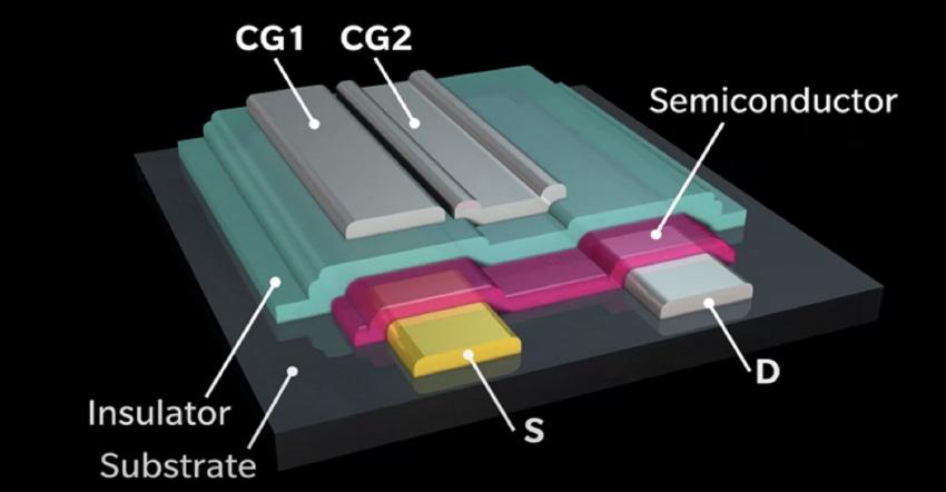
A team at the University of Surrey has developed a device called the Multimodal Transistor (MMT), which overcomes longstanding challenges of transistor design and now can perform similar operations to complex circuits.
Researchers achieved this by separating the on/off switching mechanism from the amount of current that the device puts outs, explained Radu Sporea, project lead and senior lecturer in semiconductor devices at the University of Surrey.
“Because the mechanisms are separate, one has more control over the quantity of electrons injected and the device can be designed to provide a linear dependence of output current on input voltage,” he told Design News. “The separation of mechanisms has a profound impact on many device and circuit operations.”
Traditionally, gate electrodes are used to control a transistor’s ability to pass current, which has reduced a transistor’s capacity to produce uniform repeatable signals. The MMT device overcomes this hindrance to what are called “floating gate” designs within transistors and promises efficient analog computation for robotic control, AI, and unsupervised machine learning, Sporea said.
“The device is able to perform functions which would require several components in a conventional design,” he told Design News. “This is important for emerging ultra-low-cost sensors and disposable electronics made with inexpensive manufacturing techniques, such as inkjet printing.”
Environmental Benefits
Indeed, being able to fabricate complex devices in more efficient fabrication techniques also reduces waste and the effect on the environment, Sporea said. Moreover, the MMT design also can tolerate imprecise manufacturing, so highly functional circuits can be made even with inexpensive techniques and low-performance but ecological materials, he told us.
“Applications include low-cost, flexible, and disposable medical and biological sensors,” Sporea told Design News. “Some MMT variants also allow powerful unconventional computing strategies suitable for highly efficient decision and classification operations embedded directly in such sensors. This can be achieved without resorting to complex conventional silicon chips, reducing fabrication cost and improving the end-of-life disposability of these types of devices.”
Researchers published a paper on their work in the journal Advanced Intelligent Systems.
Sporea stressed that the MMT isn’t intended to replace the conventional transistor design, but instead complement it, providing circuit designers and engineers a new tool.
The device can be used as a foundation for a number of next-generation electronic applications, including flexible displays, imaging arrays, new human-computer interfaces, lab-on-a-chip analysis tools, smart tattoos, and other wearables, and medical and agricultural bio-sensing devices, he said.
Researchers plan to continue their work to further develop the MMT, which can be manufactured alongside conventional transistors, and demonstrate applications for commercial use.
Elizabeth Montalbano is a freelance writer who has written about technology and culture for more than 20 years. She has lived and worked as a professional journalist in Phoenix, San Francisco, and New York City. In her free time, she enjoys surfing, traveling, music, yoga, and cooking. She currently resides in a village on the southwest coast of Portugal.
About the Author(s)
You May Also Like


