The Hubble space telescope in orbit.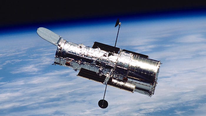
IndustryVideo: NASA Goddard's 40 Years of Non-Stop Hubble OperationsVideo: NASA Goddard's 40 Years of Non-Stop Hubble Operations
NASA's Goddard Spaceflight Center opened its control center 40 years ago.


 Closure device.")


.svg?width=300&auto=webp&quality=80&disable=upscale "Medical device software development")


.jpg?width=300&auto=webp&quality=80&disable=upscale "Tech employment prospects vary widely by state.")


Editors' Choice


Jun 4 - Jun 6, 2024
Jun 4 - Jun 6, 2024
Innovation in automation starts here. Discover and collaborate on automation solutions that are revolutionizing the entire production lifecycle — from design to production to market — and sharpen your competitive edge. ATX South is part of IME South, a six-in-one expo offering the latest insights & solutions spanning medtech, packaging, automation, plastics, design, & processing.
Register NowSign up for the Design News Daily newsletter.