Printed Transistors Can Function for Years Battery-Free
November 4, 2016

Energy harvesting is not just becoming an attractive option for wearable technology, but also for the electronic components that comprise wearable and other devices themselves.
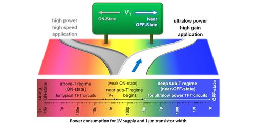
Some of the latest research in this area comes out of Cambridge University, where engineers have developed a new design for transistors that draws energy from its environment and could be the foundation for devices that can function for months or years without a battery.
The transistor generates energy from a small leakage of electrical current -- known as near-off-state current and similar to water dripping from a faulty tap -- that is characteristic of all transistors, said Sungsik Lee, a professor in the university's Department of Engineering. The method -- similar to a computer in sleep mode -- is novel because it's the first time researchers have effectively captured and used this leakage functionally, he said.

"This is the first time, and groundbreaking work, as well as unconventional thinking," he told Design News in an interview. This is because "everybody has been talking only about on-state or weakly on-state transistors, which are the conventional perception."
Another benefit to the transistors is that they can be printed on almost any material ---- such as glass, plastic, polyester, and paper -- and can be produced at low temperatures. What allows this is their unique design, which uses what is called a 'non-desirable' characteristic -- namely, the point of contact between the metal and semiconducting components of a transistor, or a so-called "Schottky barrier," Lee said.
 Enabling Global IoT/Wearables Markets. Power is a critical resource that prevents large‐scale adoption of the many billions of IoT and wearable devices that are projected to dominate our everyday lives. Intelligent power management (IPM) and Moore's Law can only reduce the power requirements so much so we are left with seemingly only two choices ... Learn more at ESC Silicon Valley, Dec. 6-8, 2016 in San Jose, Calif. Register here for the event, hosted by Design News’ parent company, UBM.
This design circumvents one of the main issues currently hindering the development of ultralow power transistors -- the ability to produce them at very small sizes. As transistors get smaller, their two electrodes start to influence each other's behavior, and the voltages spread so that below a certain size, transistors fail to function as desired.
By changing the design of the transistors, the Cambridge researchers were able to use the Schottky barriers to keep the electrodes independent from one another, so that the transistors can be scaled down to very small geometries, Lee said. "This gives a higher signal amplification of the transistor even when operating at the near-off state, or almost-off regime, helping to scale down the transistor size further while maintaining the performances," he added.
READ MORE ARTICLES ON ENERGY HARVESTING:
With the transistor's operating voltage at less than a volt and power consumption below a billionth of a watt, the component is well-suited for applications where function is more important than speed. This makes it a good fit for wearable and or implantable technology, according to Lee. "It [also] would be useful for sensor interface circuit and analog circuit in general," he said.
Lee and the team published an article on their work in the journal, Science. They aim to continue their work by demonstrating full-scale circuits and systems for wearable or implantable devices on their way to commercializing the technology, he said.
Elizabeth Montalbano is a freelance writer who has written about technology and culture for more than 15 years. She has lived and worked as a professional journalist in Phoenix, San Francisco, and New York City. In her free time she enjoys surfing, traveling, music, yoga, and cooking. She currently resides in a village on the southwest coast of Portugal.
About the Author(s)
You May Also Like

.jpg?width=300&auto=webp&quality=80&disable=upscale)

