New Material Paves Way for Smaller, High-Energy-Density Electronics
Researchers have discovered a one-dimensional material that’s highly conductive for use in high-performance electronics with very small form-factor needs.
May 16, 2018

Move over, graphene. Researchers at the University of California, Riverside, have discovered a one-dimensional (1D) material that’s also highly conductive for use in high-performance electronics with very small form-factor needs.
The material—zirconium tritelluride, or ZrTe3—can create electronics with a current density 50 times greater than conventional copper interconnect technology, according to a group of researchers led by Alexander Balandin, distinguished professor of electrical and computer engineering at the university.
To create new types of electronic material, researchers have been targeting the two-dimensional (2D) material, graphene, for its high energy conductivity. With the use of ZrTe3 to develop prototype devices with an exceptionally high current density, the exploration of new materials for this purpose moves from the 2D to 1D realm, Balandin said.
|
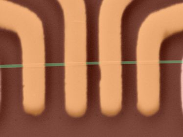
Shown is a microscopy image of an electronic device made with one-dimensional zirconium tritelluride, or ZrTe3,nanoribbons. The nanoribbon channel is indicated in green color. The metal contacts are shown in yellow color. (Image source: University of California, Riverside) |
The limitation in conventional metals has been in the fact that they are polycrystalline, he explained. This means they have grain boundaries and surface roughness, which scatter electrons. However, “quasi-one-dimensional materials such as ZrTe3 consist of single-crystal atomic chains in one direction,” Balandin noted. “They do not have grain boundaries and often have atomically smooth surfaces after exfoliation. We attributed the exceptionally high current density in ZrTe3 to the single-crystal nature of quasi-1D materials.”
Current density is the amount of electrical current per cross-sectional area at a given point. The current trend in electronic components, such as transistors in integrated circuits, is that they are becoming increasingly smaller. This means they need higher and higher current densities to perform at the level needed for an application, researchers said.
The problem with electrical conductors that have historically been used, such as copper, is that they tend to break because of overheating or other factors at high current densities. This has made them less viable for smaller electronic components, researchers said, which is why they have been seeking alternatives to materials like copper and silicon.
Graphene—a low-weight, highly conductive 2D material—has been the latest darling of nanoscale electronic component research. But that could change with the discovery by Balandin’s team, as it moves to explore as-yet untapped 1D materials for this purpose instead, researchers said.
2D Vs. 1D
2D materials consist of a single layer of atoms, while 1D materials comprise individual chains of atoms weakly bound to one another. Researchers compare 2D materials to thin slices of bread and 1D materials to spaghetti. In other words, 1D materials are much smaller than 2D materials by a significant factor.
The benefit of what are called “quasi-1D materials” is that they could be grown directly into nanowires, with a cross-section that corresponds to an individual atomic thread or chain, Balandin said. His team found that the level of current sustained by the ZrTe3 quantum wires was higher than reported for any metals or other 1D materials, reaching nearly the current density in 2D materials like carbon nanotubes and graphene.
READ ABOUT MORE RESEARCH DEVELOPMENTS HERE:
This material could serve engineers well as they develop smaller devices, as the interconnects that carry information between different parts of a circuit or system must be some of the smallest components of all. Depending on how they are configured, researchers could make ZrTe3 nanoribbons into either nanometer-scale local interconnects or device channels for components of the tiniest devices, according to researchers.
“The most exciting thing about the quasi-1D materials is that they can be truly synthesized into the channels or interconnects with the ultimately small cross-section of one atomic thread—approximately one nanometer by one nanometer,” Balandin said.
Researchers published a paper about their research in the journal IEEE Electron Device Letters. The Semiconductor Research Corporation and the National Science Foundation supported their work.
While the UC Riverside group conducted experiments with nanoribbons that had been sliced from a pre-made sheet of material, industrial applications using these materials would need to grow them directly on the wafer. Researchers already are developing this manufacturing process to promote future use of 1D nanomaterials for the development of electronics, Balandin noted.
Elizabeth Montalbano is a freelance writer who has written about technology and culture for 20 years. She has lived and worked as a professional journalist in Phoenix, San Francisco, and New York City. In her free time, she enjoys surfing, traveling, music, yoga, and cooking. She currently resides in a village on the southwest coast of Portugal.
2017 Call for Speakers INSPIRE. COLLABORATE. INNOVATE. Atlantic Design & Manufacturing, part of the largest advanced design and manufacturing industry event on the East Coast, is the annual must-attend trade show for discovering the latest in design engineering. Source from the region's most comprehensive collection of cutting-edge suppliers, deepen your expertise with free, conference-level education, and network with thousands of professionals who can help you advance your projects — and your career. From prototyping to full-scale production, one lap of the show floor will help you overcome your toughest manufacturing challenges and keep you up to speed on innovations transforming the industry. Everything you need to take projects to market faster and more cost effectively is here. Click here to register for your free pass today! |
About the Author(s)
You May Also Like


