Sign up for the Design News Daily newsletter.
ON Semiconductor Releases Highest Resolution CCD Image Sensor
ON Semiconductor has released its highest resolution Interline Transfer CCD image sensor, providing high resolution without sacrificing image uniformity and global shutter architecture.
Elizabeth Montalbano
January 25, 2016
3 Min Read
.svg?width=850&auto=webp&quality=95&format=jpg&disable=upscale "ON Semiconductor Releases Highest Resolution CCD Image Sensor")
ON Semiconductor has released its highest resolution Interline Transfer CCD image sensor, which provides high resolution without sacrificing image uniformity and global shutter architecture, the company said.
These two features are required by applications such as end-of-the-line inspection and aerial surveillance the new KAI-47051 image sensor -- an upgrade from the company’s existing KAI-29050 sensor -- is typically used for, according to ON.
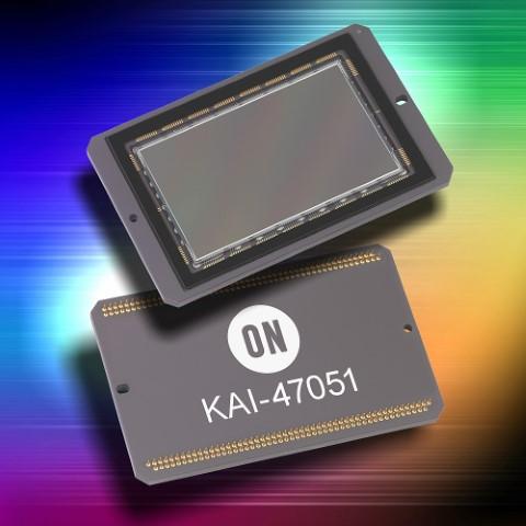
The 47-megapixel KAI-47051 image sensor increases resolution available for these applications by more than 50% compared to the KAI-29050 sensor, which is widely used by them today.
(Source: ON Semiconductor)
The 47-megapixel sensor increases resolution available for these applications by more than 50% compared to the KAI-29050 sensor, which is widely used by them today. ON specifically designed the device to be in line with the growing inspection demand for higher-resolution smartphones, tablets, computer monitors, and televisions, as well as to improve image quality and overall efficiency in surveillance applications such as aerial mapping, the company said.
The key to the design is that the sensor maintains its high resolution without losing image quality, said Michael DeLuca, go to market manager for industrial and security in ON Semiconductor’s Image Sensor Group.
[Learn more automation & control trends and developments at Pacific Design & Manufacturing, Feb. 9-11, at the Anaheim Convention Center.]
“As the resolution of flat panel displays continues to increase (from 1080p to 4k video and beyond), the imaging resolution required to inspect these devices increases as well -- requiring a new generation of image sensors that provides increased resolution without sacrificing the image quality that these applications require,” he told Design News.
CCD and CMOS are the two key technologies used to design and manufacture image sensors that both leverage the intrinsic properties of silicon to convert photons into electrons, DeLuca told us. CCD image sensors route that charge to amplifiers on the image sensor that convert the charge to voltage for external measurement, and are manufactured using a specialized manufacturing process designed for image sensors, he said.
CMOS (Complementary Metal Oxide Semiconductor) image sensors also are manufactured in a process that is also specialized, but it is leveraged from the process used for standard semiconductor processing, Deluca said. This allows transistors and logic blocks to be incorporated directly onto the sensor if desired.
[Learn more electronics trends and developments at Pacific Design & Manufacturing, Feb. 9-11, at the Anaheim Convention Center.]
Although CMOS image sensors tend to have a higher degree of functionality than CCD sensors, ON chose CCD technology for the KAI-47051 because of the very high image quality requirements of the target applications that can’t sacrifice this performance for other functionality such as increased frame rate, he said.
The KAI-47051 builds on the capabilities of its predecessor the KAI-29050 in other ways as well, according to ON. In addition to providing higher resolution by using a larger optical format, the KAI-47051 also incorporates a reduced-noise amplifier that lowers read noise by 15% compared to the previous device, increasing dynamic range to 66 decibels.
READ MORE ARTICLES ON IMAGE SENSORS:
Additionally, a 16-output architecture enables a maximum frame rate of seven frames per second, which is almost double that of the KAI-29050, the company said.
The KAI-47051 is available in a RoHS-compliant PGA-201 package in Monochrome, Bayer Color, and Sparse Color configurations.
Elizabeth Montalbano is a freelance writer who has written about technology and culture for more than 15 years. She has lived and worked as a professional journalist in Phoenix, San Francisco, and New York City. In her free time she enjoys surfing, traveling, music, yoga, and cooking. She currently resides in a village on the southwest coast of Portugal.
Like reading Design News? Then have our content delivered to your inbox every day by registering with DesignNews.com and signing up for Design News Daily plus our other e-newsletters. Register here!
About the Author(s)
You May Also Like
Editors' Choice


Jun 4 - Jun 6, 2024
Jun 4 - Jun 6, 2024
Innovation in automation starts here. Discover and collaborate on automation solutions that are revolutionizing the entire production lifecycle — from design to production to market — and sharpen your competitive edge. ATX South is part of IME South, a six-in-one expo offering the latest insights & solutions spanning medtech, packaging, automation, plastics, design, & processing.
Register Now