Additive Manufacturers Can Learn from Computer-Chip Development
Should those using additive manufacturing adopt a version of the production roadmap used by chip manufacturers?
March 10, 2022

Benny Buller, founder and CEO of Velo3D
The Additive Manufacturing (AM) industry, despite improvements, has been operating at the status quo for more than a decade. A best practice called DfAM (Design for Additive Manufacturing), created to adopt 3D printing to produce geometrically challenging parts has helped move the industry forward, but DfAM has also institutionalized and locked-in its limits. Today, confidence in AM remains stalled by such compromises.
We need to address those limits and take risks for progress. Our planet needs greater innovation in space, commercial air travel, medical devices, energy, and more. I don’t have a ready prescription for all of AM, but I’d like to share the high points of my journey to make DfAM moot and help engineers create their “impossible” products.
Discoveries from the Chip, Solar, and VC Fields
For me, the journey toward building an AM system from the ground up, and founding a company that just went public in the autumn of 2021, started in the Technology Unit of the Israeli intelligence forces. There I learned about using clean-sheet problem solving to achieve seemingly impossible objectives. The science behind that learning experience gave me a clear foundation from which to join the commercial industry.
At semiconductor-chip maker Applied Materials, I learned about the complex, layered manufacturing methods used to make computer chips—one with hundreds of steps and monitoring and control approaches. Insights gained here would lead to the deployment of sensors and test structures inside the AM system I would create.
An additive manufacturing machine is a full fabrication plant in a box. It builds the product/component from beginning to near end in a single enclosed environment. It’s similar to multi-layered semiconductor fabrication—but confined inside a single, dedicated machine. We introduced wafer-like test structures throughout our AM systems to measure and then control quality and provide us with valuable outputs. Such structures monitor, and/or help guide real-time production, managing the physics of the deposition of specific layers, chamber gases, and other factors during the AM build.
Those outputs are used to set operational parameters as well as provide feedback on worse-case scenarios. This allows validation that equipment conditions are sufficiently controlled to produce a good quality product, which is very different from just measuring the process. It addresses the unseen, surrounding physics that underly the entire additive manufacturing process.
Following Applied Materials, I joined First Solar and continued my “course work” in in-situ process monitoring and control. Many lessons were learned and goals met. We made big advances in solar module efficiency: a 50-percent improvement in solar panel power output.
After working in the Solar Industry, I moved to Khosla Ventures to learn more about the business side of startups and their markets.
Khosla Ventures was a fantastic business school. It was there that I saw the “valley of death,” a place visited by many companies whose products and technology are solely focused on replacing something at a lower cost.

Value Is Critical
Every new manufacturing technology, when invented and commercialized by a startup, has to provide its customers an added functional/performance benefit beyond lower cost. The value has to be there even at low-scale production—giving the company time to build scale and revenues gradually, ensuring also that the technology is up to the challenges of real life. This was a critical lesson I learned about bringing a new manufacturing technology to the market.
Talking with clients and experts who were exploring AM, it became clear that metal AM technology was stuck at a level of geometrical capabilities it had reached in the last century. Now, in the chip industry, Design for Manufacture (DFM) rules had continually evolved as a solution to keep driving smaller and smaller features in semiconductors even though the fundamental resolution of the lithography equipment reached a theoretical limit almost 20 years ago. But DfAM and metal AM capabilities got stuck at a geometrical limitation that was more or less frozen. These limitations are extremely harmful, design-wise, and result in massive performance compromises.
This practice of pushing a technology that doesn’t serve the customer's needs is futile. It is the reason AM adoption has been so slow. Technology cannot be pushed; it must be pulled.
Lessons from SpaceX
One of the most crucial moments for me, when I was about to establish what would become Velo3D back in 2014, came in a meeting with the propulsion and AM team at SpaceX. They told me this: "About 70 percent of the parts we try to do with AM, we produce first-shot. No issues. The supports are not an issue. Post-processing is not an issue. About 20 to 25 percent of our parts take several iterations until we figure them out. And then, with about five to 10 percent of our parts, we spend up to three months trying to produce. This includes many iterations in design, print preparation, and print parameters. But, in the end, we give up on them… If we could make this last five percent of our most innovative parts, then 100 percent of our target parts would move to this category. We would do many more parts with additive, without having to compromise or de-feature designs."
That was my “aha” moment. We now had our clean sheet and north star. The work to create our end-to-end solution started quietly in 2014 from the ground up. There were trials and failures, as there were at times in chip development, solar, and VC investment. But we reached our objectives. Our operation today is deeply customer-driven and collaborative, as it was from the beginning via that insightful talk with SpaceX.
Here Are the Lessons
In the chip industry, “Moore’s Law” projected a doubling of transistors on an IC every two years. It became a reality because of the buy-in from everyone who had a role in computing. The productivity of the AM industry will also accelerate as more lasers are added and chamber size is increased. With an improved economy of scale, costs will fall significantly, too, as they did with solar. But productivity is meaningful only if you can produce useful things. For that, DfAM, which has served for more than two decades as the official stifler of innovation, with minimal growth and evolution, must now give way to progress in manufacturing technology.
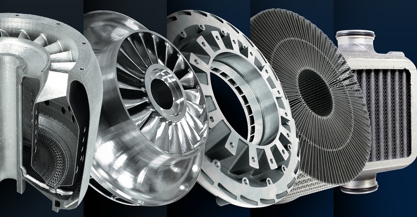
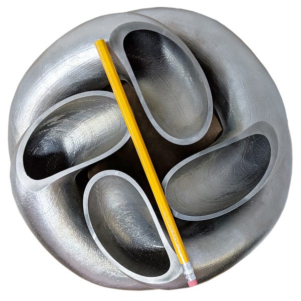
Rapid advances in chip development created a revolution throughout every sector. It changed our lives. AM can do something nearly as impressive in the area of industrial innovation, MRO, and shortened, on-demand supply chains. Advanced “support-free” AM can manufacture most blue-sky designs and create huge impacts in space and aviation, and more.
Here is where lessons, particularly from chip development—on goal-setting and accelerated improvement—can help guide us in AM. Why should we work to upend convention? To loosely paraphrase a famous idea: “Do what you think is impossible, so the impossible can then be done by others.”
Is it time to adopt a version of the roadmap used by chip manufacturers? I believe it is.
You May Also Like


