Tiniest Statue of Liberty Latest in Micro-Sized Art
The desire to place micro-sized 2D and now 3D art on objects like coins can be traced to a hidden legacy on chips and PCBs.
February 11, 2021

The Statue of Liberty has always been a symbol of friendship between the United States and France. This symbol in the form of a giant statue was first given to the U.S. in 1886. It was erected atop an American-designed pedestal on a small island in Upper New York Bay, now known as Liberty Island.
Now, a far smaller micro-scale version of the mighty giant has been created to commemorate the inauguration of President Joe Biden. The French 3-D printing specialist Microlight3D fashioned a micro-sized 1.8 mm tall replica of the famous Statue of Liberty to again honor the friendship between the two countries, as well as to showcase the company’s manufacturing prowess in using laser-based, two-photon polymerization. The company plans to use this technology for markets such as microparts and medical devices.
To break through the height limitation of existing micro-sized structures while maintaining micrometric resolution, the company used a new 3D microprinting technique known as the long-range Z feature. With this technique, they are able to 3D fabricate minute structures up to 10mm high. Previously, the height of objects was limited to 0.3mm. Increasing the height of these tiny structures is needed to create mechanical micro-parts, meta-materials, and medical devices. (Image Source: Microlight3D)
|
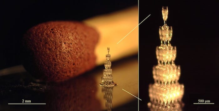
2 millimeters high Champagne pyramid. Each flute is 400microns high and contains 1nanoliter of real Champagne. |
To demonstrate that its technology is compatible with different printing substrates, Microlight3D printed the miniature Statue of Liberty directly onto the coin. The actual statue was made with OrmoGreen, a polymer doped with silica nanoparticles - the main component of glass. This polymer has shown to be ideal for making taller structures with micrometric resolution.
Two-photon polymerization technology (TPP) was used to create the 3D structures of the statue, which creates a solid 3D-printed structure from a photoactivable material. Two photons can be absorbed simultaneously by the photo-activated-monomer in the very small volume called "voxel" at the focal point of the pulsed-laser. A chemical reaction starts and the liquid monomer becomes a solid polymer inside the voxel, the company explained.
|
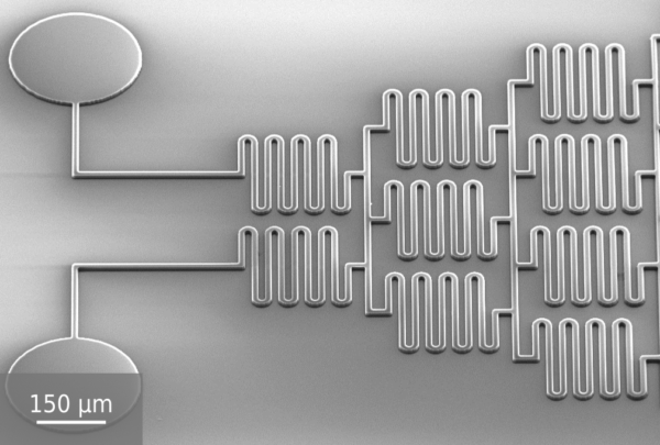
Silicon master of 20µm wide channels |
The other technique used by Microlight3D is called a Smart Print UV (SP-UV) maskless lithography system, which uses a Digital Micromirror Device (DMD) technology. This approach gives users a straightforward way to move from the design directly to the patterned sample without the use of the standard photomask fabrication. (Image Source: Microlight)
The Artist Within
The desire to create the tiniest objects and art images is nothing new. The semiconductor chip and printed circuit board (PCB) designers have been doing it as long as their respective technologies have existed. The
The Smithsonian’s Chip Art NMAH Invisible Collection on the history of integrated circuit (IC) technology contains many examples of art buried deep inside many different chips. The collection includes, “actual mask alignments, signatures and initials of the designer or perhaps the engineer and the chip art of those who have left their mark for posterity. Some are satirical quips, and some are recognizable cartoon characters.”
In 1996, the Smithsonian discovered previously unknown and hidden tiny chip art within the Integrated Circuit Engineering (ICE) Collection presented on their Chip Site. They began searching their accumulated collection of exposed chips while collaborating with Michael W. Davidson, Ph.D. - Florida State University's Optical Microscopy at the National High Magnetic Field Laboratory.
|
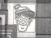
"Waldo" on MIPS Technologies R4400 Microprocessor, ca. 1994 |
Several Smithsonian collected chips have been identified and professionally photographed by Dr. Davidson and his students over the years. This collaboration is an ongoing collection of high-resolution photomicrographs (photographs taken through a microscope) featuring many of the interesting silicon creatures and other doodling scribbled onto integrated circuits by engineers when they were designing computer chip masks. (Image Source: Smithsonian, Chip Fun)
John Blyler is a Design News senior editor, covering the electronics and advanced manufacturing spaces. With a BS in Engineering Physics and an MS in Electrical Engineering, he has years of hardware-software-network systems experience as an editor and engineer within the advanced manufacturing, IoT and semiconductor industries. John has co-authored books related to system engineering and electronics for IEEE, Wiley, and Elsevier.
About the Author(s)
You May Also Like


