3D-Printing Process Creates Transparent, Flexible Circuits
Researchers in Germany have developed a multimaterials 3D-printing process to fabricate flexible circuits and other electronic components.
May 13, 2019
|
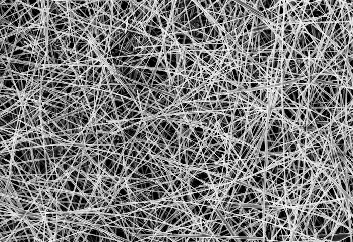
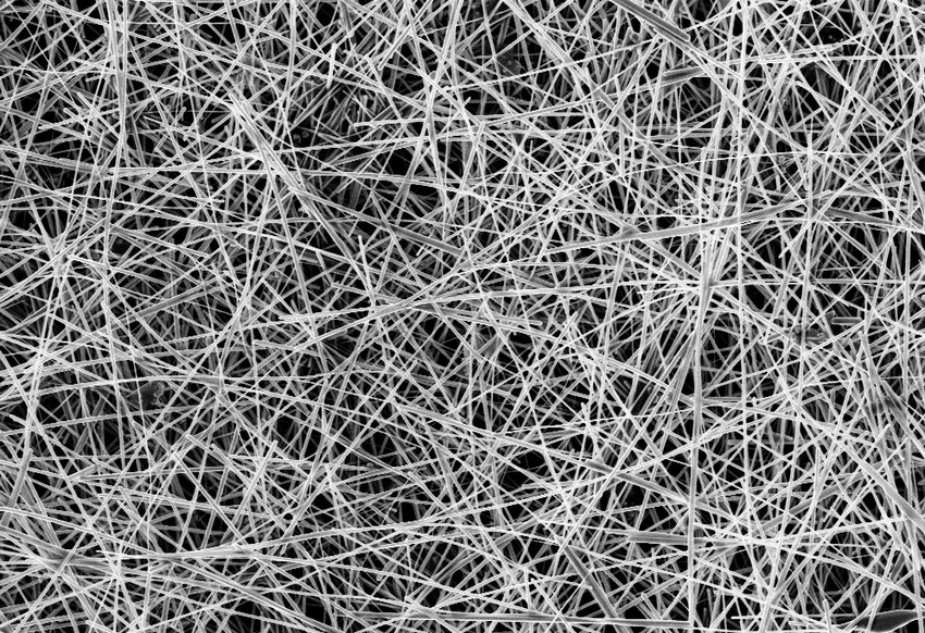
A mesh of silver nanowires forms flexible electronics created using a 3D-printing process. The wires are typically 0.01 to 0.02 millimeters long and a few dozen nanometers (millionths of a millimeter) thick. (Image source: Ferdinand Otto, University of Hamburg) |
As electronic devices move to different form factors, researchers are developing new types of components to suit their changing needs. As part of this trend, researchers at the University of Hamburg and Deutsches Elektronen-Synchrotron (DESY) collaborated to develop a 3D-printing process that can produce transparent and mechanically flexible electronic circuits.
These components can be used in new technologies such as printable light-emitting diodes, solar cells, or other tools with integrated circuits, said Professor Michael Rübhausen from the Center for Free-Electron Laser Science (CFEL), a cooperation between DESY, the University of Hamburg and the Max Planck Society.
Integrating Electronic Capabilities
“Typically 3D printing is associated with mechanical structures as the additive manufacturing process,” Rübhausen, who also is a physics professor at the University of Hamburg, told Design News. “Our intention is to integrate structure with electronic capabilities, which could be useful for many different applications related to sensing, energy storage, and computing.”
Integral to the technology that the team developed are silver nanowires—typically several tens of nanometers thick and 10 to 20 micrometers long—which form a conductive mesh within a polymer, researchers said.
As part of the process, researchers applied the silver nanowires to a substrate in suspension and dried them. They then applied a flexible polymer to the conductive tracks, which also were covered with conductive tracks and contacts.
Researchers used bright X-ray light from DESY's research light source PETRA III and other measuring methods to analyze the properties of the nanowires in the polymer to see if they achieved what they set out to do.
The detailed X-ray analysis showed that the structure of the nanowires in the polymer did not change; however, the conductivity of the mesh even improved because of the compression by the polymer, as the polymer contracts during the curing process, Rübhausen said.
RELATED ARTICLES:
Aerosol 3D Printing of Battery Electrodes
Printing a Variety of Components
To demonstrate their technology, researchers used their process to print a flexible capacitor, but said that many electronic components can be printed this way, he said.
“We are using two different polymers to show that they also can be used to tune electronics by mechanical properties,” Rübhausen added. Researchers published a paper on their work in the journal Scientific Reports.
Rübhausen said that one of the challenges researchers had to overcome in their work was that current 3D-printing technology is best-suited to printing one material at a time. Researchers, then, had to avoid clogging the printing heads due to the different materials being used, as well as to avoid contamination between printing materials, during their research, he said.
“For this, the application and embedding of the nanostructure into the composite during the printing process needs to be controlled,” Rübhausen said. The team now plans to continue its work to test how the structure of the printed objects made of nanowires changes under mechanical stress, he added.
Elizabeth Montalbano is a freelance writer who has written about technology and culture for more than 20 years. She has lived and worked as a professional journalist in Phoenix, San Francisco and New York City. In her free time she enjoys surfing, traveling, music, yoga and cooking. She currently resides in a village on the southwest coast of Portugal.
ESC BOSTON IS BACK! The nation's largest embedded systems conference is back with a new education program tailored to the needs of today's embedded systems professionals, connecting you to hundreds of software developers, hardware engineers, start-up visionaries, and industry pros across the space. Be inspired through hands-on training and education across five conference tracks. Plus, take part in technical tutorials delivered by top embedded systems professionals. Click here to register today! |
About the Author(s)
You May Also Like
