Intel Seeks to Grab More of Semi Foundry Business
Semiconductor supplier views artificial intelligence and machine learning as key markets for its expanding foundry business.

In recent years, Intel Corporation has had its struggles as the post-COVID slump in the electronics industry dealt a severe blow to the company’s core PC and server market. But not wanting to miss out on the fledgling market for artificial intelligence (AI), the company made a bold move last week by officially launching a systems foundry business.
Intel has already been growing its foundry business, which has helped sustain the company through difficult quarters during the past two years. Intel’s Foundry Services business unit posted revenue of $291 million in the fourth quarter of 2023, up 63% from the same quarter a year ago. For 2023, Intel’s Foundry Services posted revenue of $952 million, up a staggering 103% from 2022.
Given the fact Intel has already been growing the foundry services business, there would appear to be little risk in the company further expanding its footprint in this sector by establishing a sustainable systems foundry business with state-of-the-art processes and tools to capture the growth in AI chips and systems.
Willing EDA Partners
What helps is that some of the key players in IP and EDA, including Synopsys, Cadence, Siemens, Ansys, Lorentz, and Keysight, are willing partners with Intel. These companies have agreed to work with Intel to accelerate advanced chip designs on Intel 18A, which according to the company offers the foundry industry’s first backside power solution.
In addition, several vendors have announced plans to collaborate on assembly technology and design flows for Intel’s embedded multi-die interconnect bridge (EMIB) 2.5D packaging technology. These EDA solutions will ensure faster development and delivery of advanced packaging solutions for foundry customers.
Expanded Process Roadmap
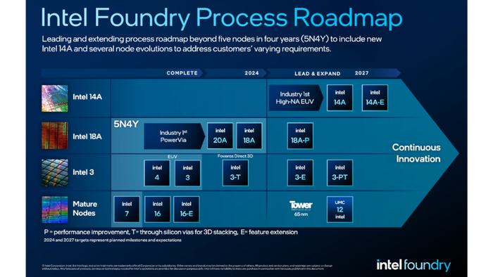
Intel’s modified process roadmap (see figure) includes evolutions for Intel 3, Intel 18A, and Intel 14A process technologies. It includes Intel 3-T, which is optimized with through-silicon vias for 3D advanced packaging designs and will soon reach manufacturing readiness. Also highlighted are mature process nodes, including new 12 nanometer nodes expected through the joint development with UMC announced last month. These evolutions are designed to enable customers to develop and deliver products tailored to their specific needs.
Intel’s extended process technology roadmap adds Intel 14A to the company’s leading-edge node plan, in addition to several specialized node evolutions. Intel also affirmed that its ambitious five-nodes-in-four-years (5N4Y) process roadmap remains on track and will deliver the industry’s first backside power solution.

Intel's latest foundry process roadmap. (Intel)
According to the company, Intel Foundry plans a new node every two years and node evolutions along the way, giving customers a path to evolve their offerings on Intel’s process technology continuously.
Intel also unveiled an "Emerging Business Initiative" that showcases a collaboration with Arm to provide cutting-edge foundry services for Arm-based system-on-chips (SoCs). This initiative allows Arm and Intel to support startups in developing Arm-based technology and offering essential IP, manufacturing support, and financial assistance to foster innovation and growth.
Samsung, GlobalFoundries Make Moves Too
While Intel made the bulk of the noise in the foundry services business, other semiconductor and foundry service companies are not standing still.
Seeking to strengthen its presence in AI, the Korean electronics supplier announced a collaboration with Arm to deliver an optimized next-generation Arm® Cortex™-X CPU developed on Samsung Foundry’s latest Gate-All-Around (GAA) process technology. This initiative is built on years of partnership with millions of devices shipped with Arm CPU intellectual property (IP) on various process nodes offered by Samsung Foundry.
The collaboration will set the stage for a series of announcements and planned innovations between Samsung and Arm. The companies plan to reinvent 2-nanometer (nm) GAA for next-generation data center and infrastructure custom silicon, and an AI chiplet solution aimed at the future generative artificial intelligence (AI) mobile computing market.
Also, U.S. pure-play foundry GlobalFoundries announced it would expand its Malta, NY plant by adding critical technologies already in production in GF’s Singapore and Germany facilities geared towards enabling the U.S. auto industry. The company expects this expansion will help ensure supply chain resilience to meet the growing demand for chips used in AI, aerospace, and defense.
GlobalFoundries will also update its 200mm facility in Essex Junction, Vermont. The project will expand capacity and create the first U.S. facility capable of high-volume manufacturing of next-generation gallium nitride (GaN) semiconductors for electric vehicles, power grids, data centers, 5G and 6G smartphones, and other critical technologies.
About the Author(s)
You May Also Like


