

Sign up for the Design News Daily newsletter.
Startup company Atomera believes its silicon enhancement technology can help semi makers optimize power management chip cost and performance, without having to upgrade production processes.
3 Min Read

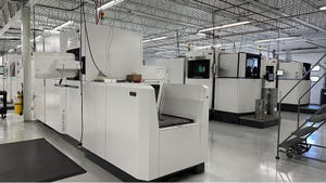
Startup company Atomera said its silicon enhancement technology can help optimize chip performance, size, and cost without having to invest in upgrading manufacturing processes. Image courtesy of Image Source / Alamy
For many years, the common assumption with Moore’s Law is that going to a new manufacturing node would typically result in power, performance, and cost improvements of 20% or greater, assuming appropriate capital expenditures for new equipment and processes are made. But startup Atomera is challenging that assumption with a patented silicon enhancement technology it believes would enable semiconductor makers to reap many of the same benefits, without the costly capital expenditures.
Founded in 2016, Atomera is headed by President and CEO Scott Bibaud, a semiconductor industry veteran. In an interview with Design News, Bibaud said the materials technology, called MST, has been in development for over 15 years. Given existing chip shortages and the long payback period for capital expenditures, Bibaud believes the technology could help mitigate chip capacity issues and rapidly escalating wafer prices, by enabling semiconductor manufacturers to leverage existing fab equipment and processes.
“Previously, it always made sense to redesign a chip to go to a new process node,” said Bibaud. “But a new node is costly and capital expenditures can be substantial.”
Bibaud added that Moore’s Law used to dictate at least a 20 to 25% improvement in PPAC (power performance area cost). But as PPAC payback from process node changes starts to level off, the economics of costly capital expenditures come into question.
Standard Manufacturing
Atomera’s solution is a quantum-engineered material, called MST (Mears Silicon Technology), that is deposited during the chip manufacturing process. What makes the technology relatively economical to implement is the fact that it can be implemented on standard manufacturing tools, without the user having to incur significant additional capital costs or modification of semiconductor fabrication processes.
While Bibaud believes the technology can be adapted for many types of semiconductors, he expects Atomera’s initial trust will focus on enhancing 5V transistor technology for power management chips, where many legacy parts exist. In the power management sector, power devices can be up to 80% of the power management IC die area, and process nodes typically range from 40 nm to 250 nm.
“The technology enables the design engineer to optimize speed, cost, and power,” Bibaud said. He explained that with the material, engineers can use it as is to make the circuit run faster, reduce costs by shrinking the transistor until the drive currents match, or reduce voltage until drive currents match. The materials technology can be optimized to trade off speed, cost, and power requirements to suit the product being developed, Bibaud noted.
According to Bibaud, the MST technology enables to improve PPAC factors by at least 15%, which would compare favorably with PPAC improvements derived from costlier process node upgrades.
The cost improvements, Bibaud noted, lie in the process efficiencies of obtaining more, smaller dies from wafers, improving chip yield and thus profitability. Even a 5% die shrink for a 36 mm2 die would result in at least 5% more die per wafer, and the yield would increase as die size shrinks, according to him.
Bibaud cited the example of applying the MST technology to a typical power management IC used for a high-volume mobile phone application. He noted that a 20% die shrink could typically result in 10% higher gross margin for the chip.
The company has recently made several moves to implement the materials technology, including entering a joint development agreement with a major, unnamed silicon foundry. Bibaud added that Atomera is currently engaged in discussions with 19 companies on licensing and further developing its technology.
About the Author(s)
You May Also Like
Editors' Choice


Jun 4 - Jun 6, 2024
Jun 4 - Jun 6, 2024
Innovation in automation starts here. Discover and collaborate on automation solutions that are revolutionizing the entire production lifecycle — from design to production to market — and sharpen your competitive edge. ATX South is part of IME South, a six-in-one expo offering the latest insights & solutions spanning medtech, packaging, automation, plastics, design, & processing.
Register Now