The performance advantages of wide bandgap power semiconductors are driving their design in growing apps for EVs, data centers, and consumer devices.
December 27, 2022
Patrick Waurzyniak
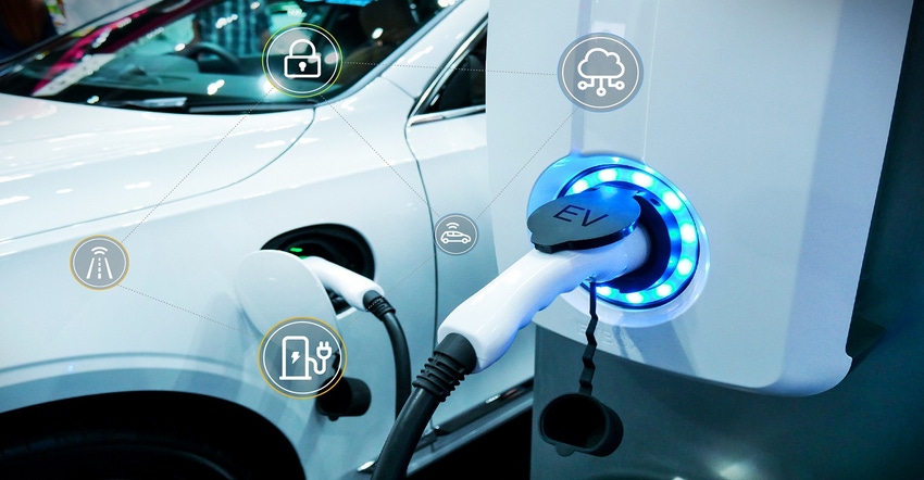
Silicon carbide (SiC) and gallium nitride (GaN) power semiconductors are projected to hit record growth levels, spurred on by the latest applications for power ICs, particularly those in battery electric vehicles (BEV), such as traction inverter and on-board applications, as well as for consumer electronics battery chargers, datacenter apps, and energy infrastructure applications.
After the pandemic downturn, power IC makers are investing heavily in new plant and manufacturing technologies for both SiC and GaN production. Semiconductor analysts had expected the SiC and GaN power IC market to pass the $1 billion in 2021, according to a 2020 Omdia research report, but the wave of current investment is likely to drive growth in the wide band gap (WBG) SiC and GaN semiconductor markets even higher.
SiC-based design wins have multiplied for electric vehicle applications and will drive the SiC market beyond $2.5 billion by 2025, noted Lyon, France-based Yole Développement in its November 2020 report. For power GaN devices, Yole’s Power GaN 2022 report, released in June, forecast the power GaN market to be worth US$2 billion in 2027, with consumer devices, including power supplies and Class D audio amplifiers, representing 48% of the total GaN market in 2027.

“GaN fast chargers are growing rapidly in the handset market. Since 2020, Yole has seen an increasing number of fast chargers featuring GaN devices from players such as Power Integrations, Navitas, and GaN Systems,” said Taha Ayari, technology and market analyst, Compound Semiconductors at Yole: “Now Innoscience is also contributing to this market with high volumes.”
Manufacturers are bumping up their investments in SiC and GaN to meet expected demand. In September, Wolfspeed announced a new multi-billion silicon carbide materials facility in Chatham County, North Carolina, to build primarily 200mm SiC wafers, which are 1.7x larger than the 150mm wafers, translating to more chips per wafer and lower device costs. The investment eventually will generate a 10-fold increase in Wolfspeed’s currently SiC production capacity at its Durham, North Carolina headquarters campus. The new wafers will be used to supply the company’s Mohawk Valley Fab in Marcy, NY, which opened earlier this year and is what the company called the largest and only fully automated 200mm SiC fabrication facility.
In August, Navitas Semiconductor, the El Segundo, Calif.-based maker of GaN power ICs, acquired GeneSiC Semiconductor, a pioneer in SiC design and processes, for approximately $100 million. The deal positions Navitas, maker of the GaNFAST line of power ICs, as a pure-play, next-generation power IC manufacturer with both GaN and SiC lines for fast-charging in EVs and data centers.
Choosing SiC or GaN?
The advantages of WBG compound semiconductors like SiC and GaN over standard silicon are numerous, although costs for these new devices initially will be higher, analysts say. For lower-voltage applications, like chargers and consumer devices, GaN will be the choice for 650 V and under, while higher-voltage requirements like electric vehicles often dictate using SiC devices capable of handling 800 V and above.
“With respect to the EV market, a key trend is the transition from 400 V to 800 V batteries, which enable higher efficiency (longer range or reduced battery size for same range), faster charging, and overall cost reductions,” noted Victor Veliadis, executive director and chief technical officer for PowerAmerica, in Raleigh, N.C. “This transition makes the SiC proposition stronger with respect to Si and GaN. 1200 V SiC MOSFETs have been commercially available since 2011 and have gone through several generations of optimization from many suppliers. A 2 level inverter topology can be implemented with 1200 SiC transistors to address 800 V EVs.”
Examples of these higher-voltage EVs include the Porsche Taycan, Audi Q6 e-tron, Hyundai Ioniq 5, and Lucid Air, with 800 V or higher voltages offering longer range/higher efficiency and faster charging.
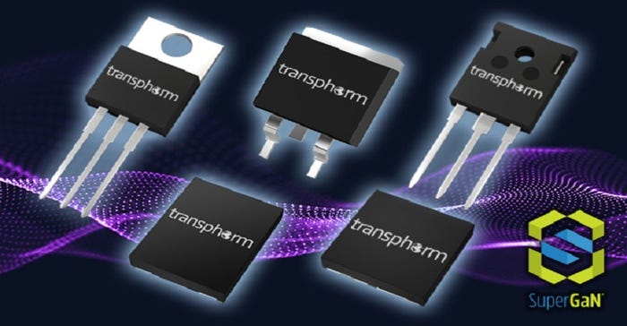
Commercially available GaN is primarily at 600 V, with one company, Transphorm, offering a 900 V product, Veliadis noted. “An 800 V battery GaN-based inverter is implemented with a 3 level topology that requires double the number of devices vs. 2 level. 2L (SiC) uses fewer devices than 3L (GaN) and has lower control complexity. On the other hand, 2L suffers higher output voltage harmonic distortion. So GaN is competing with SiC for 800 V battery EVs and several projects are looking at 2L (SiC) vs 3L (GaN) advantages/disadvantages and overall bill of materials costs.”
Automotive the Killer App for EVs
For now, SiC is seen by far as the better alternative power IC over GaN chips for high-power, high-voltage automotive applications. “SiC, being more mature than GaN, and better suited for the high voltage and high powers of EV inverters, will continue to make design wins in the mainstream 400 V battery and the emerging 800 V battery EVs,” Veliadis noted. “GaN will continue to compete at 400 V successfully, and build a proposition for 800 V EVs. The onboard charger requires lower power levels compared to the traction inverter, and so GaN is a very competitive solution for that application.”
For traction inverters, the adoption of 800 V batteries is expected to accelerate, said Jonathan Liao, senior product line manager, VE-Trac, for Phoenix, Ariz.-based power IC maker onsemi. Besides Lucid, Porsche, Audi, HKMC, additional manufacturers such as BYD, BJEV, BMW, are expected to transition from 400 V to 800 V batteries in the next two to three years, Liao added.
SiC is expected to grow at a 39% CAGR between 2022-2029, said Liao, adding that Onsemi believes the growth rate will further accelerate, especially in traction inverter applications. “Many traditional OEMs and disruptors alike are trying to catch up in technology to the EV market leader Tesla, which uses SiC in most of their traction solutions to gain efficiency, higher performance, and better reliability. EVs with SiC traction solutions offer longer range, faster acceleration, and improved lifetime.”
For 2023 and beyond, George Liang, director, Product and System Application Engineering at Infineon, said he expects semiconductor companies to bolster capital investment in SiC manufacturing capacity due to increasing demand for the devices for EV power train, charging and energy storage. “Learning from the supply chain constraint issue in 2022, electric vehicle makers will push harder to semiconductor companies on the second source and application design compatibility requirement for SiC devices,” he said. “This will drive the standardization of SiC packages.”
Liang added that semiconductor companies will speed development of new SiC and GaN devices with lower Rds,on and better package technology for thermal conductivity due to increasing power and density requirement for inverter and charger applications fast charging. “Moving from 6-inch to 8-inch wafer diameters will become necessary to increase capacity and lower manufacturing cost for SiC WBG devices,” Liang said.
Infineon and Stellantis in November announced a non-binding multi-year deal for the chipmaker to supply Stellantis with its SiC chips for EVs, with Infineon reserving manufacturing capacity and supply of its CoolSiC “bare die” chips in the second half of the decade to direct Tier 1 suppliers of Stellantis. In 2024, Infineon’s new SiC fab will open in Kulim, Malaysia, complementing existing manufacturing capacities in Villach, Austria.
Silicon carbide is well-established in the EV market today, noted Henning Hauenstein, VP of Strategy at NXP, and while it’s more expensive than traditional silicon, it offers efficiency improvements that make the tradeoffs worthwhile. “For example, it might enable an OEM to use a smaller EV battery or deliver a longer-range vehicle,” Hauenstein said. “These system-level benefits mean that we expect to see continued adoption of SiC in 2023, with manufacturers working to build capacity to meet that need.” Outside of the automotive market, he said “SiC’s high-voltage capabilities make it well-suited to energy transformation, power grid, or heavy-industry applications.”

Lowering Costs, Defect Rates
Key hurdles chipmakers face with newer processes include obtaining adequate chip yields and lowering the defect rates in chip substrates. Moving to larger 200mm wafers further complicates the equation. “This is certainly a challenge. SiC is the more mature and robust technology at this point, but there are still challenges for both SiC and GaN around growing high-quality wafers with a low defect density,” Hauenstein said. “One trend is to repurpose some of the legacy fabs that were being used to manufacture older technologies and convert them to make these power devices instead.”
In SiC, the substrate synthesis process is very labor-intensive and involves temperatures in the 2300-2500 °C range vs. 1500 °C for silicon, notes PowerAmerica’s Veliadis. “SiC boules are smaller in length and take longer times to form. The wafering process is more complicated, and a deep learning curve is needed to form single polytype (4H) SiC wafers with low defectivity,” Veliadis explained. “Furthermore, many SiC fab processes require specific equipment not available from the Si world. Apart from the starting wafer defects, one can generate defects during SiC processing, particularly during the high-temperature implantation and subsequent ~1600 °C anneal.”
Another issue is the lower planarity of SiC wafers compared to Si, which complicates their processing, particularly as the epitaxy thickness increases to achieve high voltages, Veliadis said. “The presence of defects dictates the optimal SiC device area beyond which yields drop unacceptably,” Veliadis said. “Engineers are working on these issues improving material quality and flatness, and optimizing fabrication alongside Si to exploit economies of scale. Today, wafer quality and fabrication are sufficient to produce good yields at specific device areas.”
The cost of SiC devices will be more expensive than those of Si, if substrates continue to be produced with “conventional” methods, even when the economies of scale that EV is bringing are taken into consideration, he said. “However, the efficient operation of SiC and GaN devices at high frequency brings system simplifications like lower weight and volume, simplified thermal management, and reduced size/weight of passive components like capacitors, inductors, and transformers. As a result, SiC cost savings at the system level make the technology competitive with Si and outweigh the higher cost of manufacturing SiC devices,” Veliadis said. “Moreover, this parity is before taking into account the energy savings over the lifetime of the system. This is the case with SiC in photovoltaic systems and increasingly so in EV and other applications.”
Commercially available lateral GaN power devices are made on low-cost Si substrates, Veliadis pointed out. “Lateral GaN power devices are CMOS compatible and fabricated in large volume fabs like TSMC using mature nodes, thereby enabling Si economies of scale manufacturing.”
GaN’s Expanding Potential
The relative ease of GaN’s manufacturing process and broad application scope can make it appear to be a more attractive value proposition for power IC makers. GaN and SiC focus on different voltage nodes and applications, noted Alex Lidow, CEO and co-founder of Efficient Power Conversion (EPC), a GaN manufacturer based in El Segundo, Calif. “In my opinion, GaN is better than any other technology at 650 V and lower,” Lidow said. “SiC is better than any other technology at 900 V and higher. GaN, SiC, and silicon all compete in the 650 V–900 V space, which includes automotive applications, so I think we’ll find out over the next few years which technology prevails in this battleground area.”
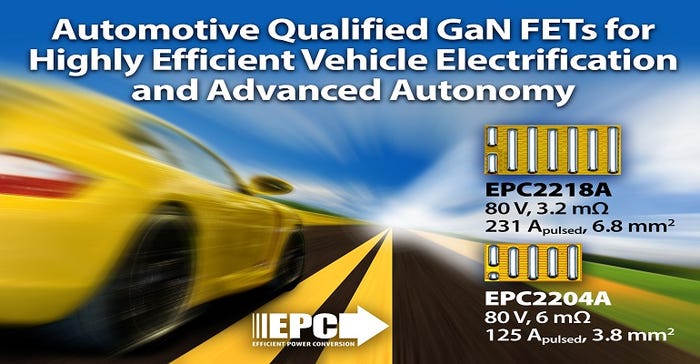
The key technology trend to watch for with GaN devices is the evolution from discrete to highly integrated solutions, Lidow noted. “EPC started integrating devices more than seven years ago with monolithic half bridges and has subsequently expanded to add more features and functions. Monolithic power stage ICs perform all the same functions as a multi-chip DrMOS module based on silicon MOSFETs, but at higher voltages, higher switching speeds, in a smaller footprint, and at lower cost,” he said.
The most common misconception about GaN technology is that it costs more than silicon, Lidow said. “In about 2015, the first GaN-on-Si transistors started shipping that were actually lower in price compared with Power MOSFETs with the same on-resistance and voltage ranges.” Since then, GaN transistor prices have continued to decline, he noted, while at the same time, the technology has improved, and die-shrinks have been achieved.
Old legacy silicon is being replaced by SiC and GaN in many power semiconductor applications, said Stephen Oliver, vice president, marketing and investor relations for Navitas Semiconductor. By adding the GeneSiC power IC line, the company can now target the full EV line, with SiC and GaN chips used manner of EVs from scooters to 18-wheelers, Oliver said.
Navitas’ GaNFAST line of chips are designed by the company but built at its fabrication partner, X-Fab in Lubbock, Texas. “We don’t make them, but what we do is we understand the limitations of the processes and design around them,” Oliver said. “We can actually get more of the process than others can.” For SiC chips, Navitas’ yields start at about 90%, whereas the industry standard is starts at 70-80%, and for its GaN line, the company achieves 90-95% yields typically, he said.
GaN devices are on the rise, especially for higher-power applications in data centers, UPS/energy, PV inverters, industrial, gaming power, to name a few, noted Primit Parikh, co-founder, president and COO of GaN chipmaker Transphorm Inc. “On the R&D front, Transphorm is working on advances like 1200 V GaN and a bi-directional (four quadrant) GaN switch, a unique device enabled by lateral GaN.”
Parikh sees GaN’s opportunity continuing to expand, compared to SiC. “High-voltage GaN technology is being adopted at an increasingly faster rate. Notably, Transphorm’s customer applications are running the gamut—from low-power adapters through to 4-kW+ industrial power supplies among other applications.”
Higher voltage and power capabilities characterize the latest GaN devices. “We are the first GaN manufacturer to add a 900 V device to our 650 V FET portfolio,” Parikh pointed out. “The 1200 V GaN platform is now in development, which truly positions it as a universal technology capable of supporting the broadest spectrum of power levels, from 45 W to 10 kW and higher. We’ve really only begun to tap into GaN’s potential.”
You May Also Like
