Imec developing virtual model that will demonstrate optimal processes for environmentally sustainable semiconductor manufacturing

The semiconductor industry is a big user of resources such as electricity and water and utilizes potentially polluting materials such as chemicals on its production lines. As they look towards the future, more semiconductor companies are taking a long look at their environmental footprint, including their manufacturing processes, with an eye toward lower greenhouse gas emissions.
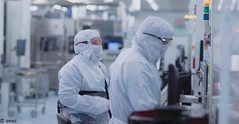
Imec, an R&D and innovation hub for nanoelectronic and digital technologies, is developing a model for green manufacturing. The company has initiated a project that seeks to develop a blueprint of sustainable semiconductor manufacturing techniques for key processes such as lithography and etching.
To achieve this, Imec has established a “virtual fab” to demonstrate its strategies to reduce the carbon footprint from semiconductor process steps. “We are working with pieces in the value chain to create a virtual fab,” said Emily Gallagher, Principal Member of Technical Staff at Imec, in an interview with Design News. “We want to examine the environmental impact of different semiconductor process steps such as lithography.
The virtual fab involves a massive quantitative assessment of the environmental impact of patterning in advanced IC manufacturing. Using its imec.netzero modeling platform, Imec has quantified the environmental impact of patterning-related process steps for various logic technology nodes.
Through the ‘virtual fab’ tool, Imec has shown that lithography and etch together are responsible for 45 percent of the Scope 1 and Scope 2 emissions (i.e., emissions from owned or operated assets, and from purchased energy, respectively) associated with fabricating 3nm logic wafers. According to Gallagher, the virtual fab will enable imec and its foundry and semiconductor vendor partners to assess their current footprints for green manufacturing.
Examining Tradeoffs
Gallagher noted that using the modeling tool to emulate a fab makes it easier for Imec to explore the tradeoffs of using, for example, different amounts of extreme ultraviolet lithography (EUV) in fab processes and measure their impact on carbon dioxide emissions. These measurements become extremely crucial as the industry moves from 10 nm to 7 nm and then to 5 nm process patterns for future semiconductor fabrication, Gallagher added.
Not all the research is virtual. Imec is still using its physical fab to explore process and design solutions for the high impact areas, which include the reduction of fluorinated etch gases, maximizing EUV scanner throughput, and reducing hydrogen and water consumption.
Recently, Imec installed a hydrogen recovery system for EUV lithography in its 300 nm cleanroom, which Gallagher said enabled the company to recover 70% of the hydrogen.
Industry Efforts
Major semiconductor and electronics companies have in recent years made major efforts to improve environmental sustainability, as a way of doing business.
Intel, for instance, sends sulfuric acid wastes from manufacturing operations to an off-site facility, where it is turned into technical-grade sulfuric acid that is used on onsite wastewater treatment. The company also segregates the constituent parts of its spent solvent waste to make it easier for waste vendors to refine high-value solvent and resell it as a raw material. This helps reduce fossil fuel consumption.
Another major electronics supplier, Apple has implemented a host of recycling and energy-saving measures at its various facilities. For production, Apple conducts constant testing of materials for health and environmental impact. It has also moved to using environmentally friendlier cleaners and degreasers.
“All of these companies have net zero emissions objectives,” Gallagher noted. She believes environmentally-sound manufacturing will become a business advantage as electronics production evolves to meet future needs.
“Tool suppliers with greener options will have advantages,” Gallagher said.
Spencer Chin is a Senior Editor for Design News covering the electronics beat. He has many years of experience covering developments in components, semiconductors, subsystems, power, and other facets of electronics from both a business/supply-chain and technology perspective. He can be reached at
About the Author(s)
You May Also Like


