June 26, 2013

Midwest industry is likely to get a big next-gen boost by a new project in northeastern Ohio that is embracing the future.
Instrument and controls is a manufacturing sector that includes sensory and measurement tools along with the motors and actuators that are activated by the readings of those devices. This industry makes up 50 percent of the total industry found in Ohio, and accounts for about $100 billion worldwide. A new, multi-user, shared resources facility has opened in Elyria, Ohio at the Lorain County Community College that is open to entrepreneurs, established companies, inventors, and students looking to prototype, produce, and sell microsystems.
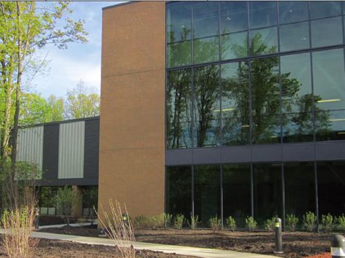
Many useful resources specific to this type of production are now found at the new Richard Desich SMART Center for Commercialization of Microsystems.

The 46,270 sq. ft. building is fully equipped for microsystems reliability testing, analysis, inspection, and packaging. Nine thousand sq. ft. of the center will be made up of "class 10,0" and "1000" (ISO 7) cleanrooms, and numerous pieces of equipment are available for use by anyone for an hourly rate. The lab is completely dedicated to quick production and testing of microsystems, micro electrical mechanical systems (MEMS), semi-conductor devices, and commercial sensors. These devices require high-cost, highly-specialized tools, which can deter small or established businesses from innovating. At the same time, it is these devices that will undoubtedly be at the heart of numerous electronic, medical, and environmental applications.
One could imagine that containing MEMS and preparing them for distribution would be a difficult task. Microsystems packaging tools include a washing station, die saw, wire bonder, plasma chamber, curing ovens, micro printer, stencil printer, plasma cleaning, flip chip, aluminum wedge bonding, gold stud bumping, epoxy lid sealing, and gold ball bonding, to name a few.
Reliability testing can be done using temperature and humidity chambers, thermal shock tests, UV tests, HAST chamber, electrodynamic shakers, accelerated UV weathering, shear and tensile tests, thin film metrology, and more.
The tools to do these tasks come from quality companies that have collaborated with the SMART Center. Zygo, Cascade Microtech, Leica, Labworks Inc., and Nordson are a handful of contributors whose machines are available at the Desich Center.
Connectivity and interfaces between micro systems to other field components are standardized and overseen by the Field Device Tool Technology Group, an affiliate of the project. The SMART center's Sensor Integration and Technology Testing (SITT) will be the first in the Americas to be authorized for testing and evaluating devices and interfaces, and determining their compliance with FDT standards.
For the all-important inspection and characterization of micro components, there are 3D optical profilers; an electrical probe station; acoustic, light, and stereo microscopes; thin film metrology; surface profiling; film stress analysis; and thermal imagers including a near-IR imager. The equipment available is sophisticated enough to make systems and devices compliant with Mil-Spec, ANSI, and JEDEC standards.
Once an individual or organization finishes a prototype wafer, experienced engineers and technicians can help with the project's development. Advanced development and simulation software has been developed specifically for SMART Center users. This exclusive software suit is capable of MEMS design, mask layout, linear, and non-linear FEA, and solid modeling.
It's safe to say the facility will produce many supporters as it will micro systems. This will not be the last organization of its kind that we see, but it is a courageous effort that will seem obvious in hindsight. The center and all its contributors are working to reduce the cost and risk of commercializing MEMS and sensor technology that will be at the heart of the growing (but shrinking) electronics and nano-tech industries.
Related posts:
About the Author(s)
You May Also Like


