Image a reality where molecular robots manufacture precise atomic structures to help cure cancer and change the course of semiconductor fabrication. It's here!
January 28, 2020

Over the last few years, global competition and technological advances have focused much attention on the areas of additive manufacturing, 3D printing, smart manufacturing and the like. What has often been neglected are the advancements on a different kind of manufacturing, one where the production floor is only a few nanometers in height. In this world, molecular assemblers scurry across a tiny floor to assemble structures with atomic precision – i.e., atom by atom. This is the reality that the famous physicist Richard Feynman hinted at when he talked about a way to “arrange atoms the way that we want.”
The ideas and initial advances in nanometer technology were significantly influenced by Eric Drexler, an MIT graduate best known for his studies in molecular nanotechnology. Unlike conventional chemistry, in which molecules react as a large group, Drexler proposed a method of "mechanosynthesis" in which individual molecules were specifically positioned close together so that stronger chemical attractions could occur in a controlled way. With such atomic precision, atoms could be added or removed from a structure as desired.
In his book – Engines of Creation: The Coming Era of Nanotechnology – Dr. Drexler proposed the concept of nanoscale assemblers that would build copies of themselves and other molecular sized objects with atomic control. From this, a microscopic production line could be created to build larger and more complex structures, even products that connect to today's semiconductor devices.
There are many examples of such production lines in our world today. Recently, scientists have been able to show how tiny autonomous bots could function as intelligent delivery vehicles to cure cancer in mice. It is even possible to fabricate functional DNA nanostructures that include logic gates to deliver and release molecular cargo for medical applications. Other feasible molecular machines include the molecule walker and the smallest nanocar, which has wheels driven by electronic tunneling.
One new area where atomically precise manufacturing (APM) shows great promise is in quantum technologies, where energy levels and quantum tunneling transport are extremely sensitive to single atom dimensions. APM would be an order of magnitude more precise than even today's leading edge e-beam semiconductor lithography techniques.
A few year ago, I had the opportunity to talk with Dr. Eric Drexler about nanotechnology, atomically precise manufacturing and its relationship to current semiconductor lithography approaches. What follows is an edited version of the actual conversation, part of the Linus Pauling Lecture Series.
|
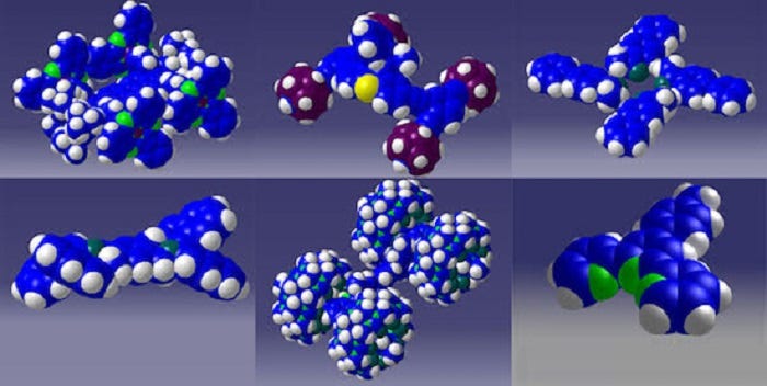
Image Source: CEMES - CNRS |
Design News: In the world of semiconductor technology, one tends to think of nanotechnology in terms of leading-edge geometric nodes, Moore’s Law scaling, lithography and the like. How do you define nanotechnology?
Eric Drexler: I think that the word nanotechnology has a very large range of appropriate meanings. It's used for everything from fine grained materials through concepts for future manufacturing and should be used more than it is in describing semiconductor technology today. The most impressive nanotechnology in the world today is the nanotechnology that you find in your pocket of billions of devices that are down in the range of tens of nanometers and scale that are the basis for the information revolution. It's only a matter of history and marketing that makes people ask; “what is nanotechnology given us?” Well, the answer is information technology in its modern form.
Design News: In talking about nanotechnology you emphasized that the biological approach was perhaps a little less useful than the mechanical or engineering fabrication approach. Would you comment on that?
Eric Drexler: The kind of nanotechnology that by the nature of things has to be the future is one with atomic precision. Down at the nanometer scale, structures are only a few or a few tens of atoms in diameter. To get the full potential of such technologies requires having the building blocks arranged with precision. Now it turns out that that is already done very widely in the world today. We have a very powerful technology of atomically precise fabrication. It has been in existence for more than a century and is called organic synthesis. It has now developed with aid from biological technologies to be able to support the design and fabrication of structures of with millions of atoms and on a scale of hundreds of nanometers. So today, the electronic devices that are made from the top down of using light, etching and lithographic technologies are making smaller features than the scale of the atomically precise structures that are now made. So these bottom-up (atomically precise) and top-down (lithographic) technologies are now in an overlapping size range and there is reason to believe that they can be integrated to make a very interesting generation of further extensions of our nano-electronic technology.
Design News: At 14 nanometer and below, they are starting to talk about double patterning and directed self-assembly. Is that an example of what you're talking about?
Eric Drexler: Here's an example of what I think is likely to be feasible and may in fact be done. In the molecular sciences, when someone makes components, they don't make one they tend to make hundreds of billions of them at once because you work with many, many, many molecules together. Device down in the range of a moderate number of nanometers our structures of that kind if they have the right structure will form crystals. They'll stack up systematically in a spontaneous way. So imagine a semiconductor chip patterned at 14 nanometers or perhaps better with addressing logic in that semiconductor substrate and a regular array of addressable locations on the surface. Now integrate the structures such that you can grow a crystal of macromolecular structures on top of that perhaps a thousand layers deep. The prospect is having something that has the area density of present-day flash memory but instead of stacking cells a few high, you stack them a thousand high and without adding a thousand process steps. Instead having a moderate number of process steps to make the base layer where the complexity is and then using the physical principles of crystal growth to make the layers on top.
Design News: The issue then would be one of interfacing because you’d still need to interface to the outside world. Is that correct?
Eric Drexler: Well, in this picture, the interface is exactly the semiconductor chip. What you have is something very similar to an existing flash memory in the sense of having address logic in the semiconductor side. All that is being done at the on the molecular side is a regular array and you already see regular arrays in memory. But building up from the semiconductor addressable array to many layers where the addressing would now go through those layers to address points in the interior. So the complexity is all offloaded to where people do complexity well today which is with lithography.
Design News: One final question: In your talk you kind of outline the necessity for and the structure for a molecular systems engineering. Would you touch on that briefly why it's needed?
Eric Drexler: In the world of science and technology today, there is a lot of capability to do atomically precise fabrication, i.e., synthesizing molecules that will self-assemble on a scale of up to millions of atoms. What is needed to make the kind of progress that I think will have the greatest long-term effect, is to take those kinds of capabilities – i.e., different kinds of molecules and different self-assembly processes – and put them together the way that engineers put things together. By that I mean to, design components that fit particular functional roles in a systems architecture and that fit functional roles and fit together physically and build complex systems. In the sciences today they're structured to make discoveries and structure to in many cases develop application in biology. The need is to take those same tools for atomically precise fabrication and do organized system development that can make for example machines that work a lot like a 3D-printer but organized atomically precise blocks instead of bits of plastic and metal.
|
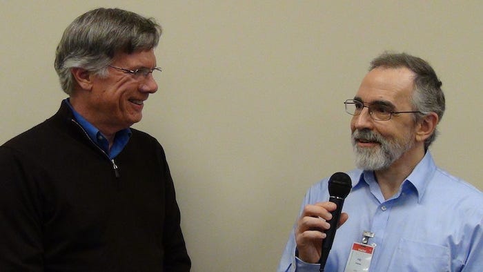
Image Source: Linus Paulin Lecture Series / John B |
John Blyler is a Design News senior editor, covering the electronics and advanced manufacturing spaces. With a BS in Engineering Physics and an MS in Electrical Engineering, he has years of hardware-software-network systems experience as an editor and engineer within the advanced manufacturing, IoT and semiconductor industries. John has co-authored books related to system engineering and electronics for IEEE, Wiley, and Elsevier.
About the Author(s)
You May Also Like


