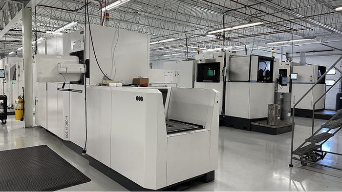
ultrasonic metal welding GMX Micro D Type.jpg?width=700&auto=webp&quality=80&disable=upscale)
ManufacturingUltrasonic Metal Welding Evolves to Meet Energy Storage System Manufacturing NeedsUltrasonic Metal Welding Evolves to Meet Energy Storage System Manufacturing Needs
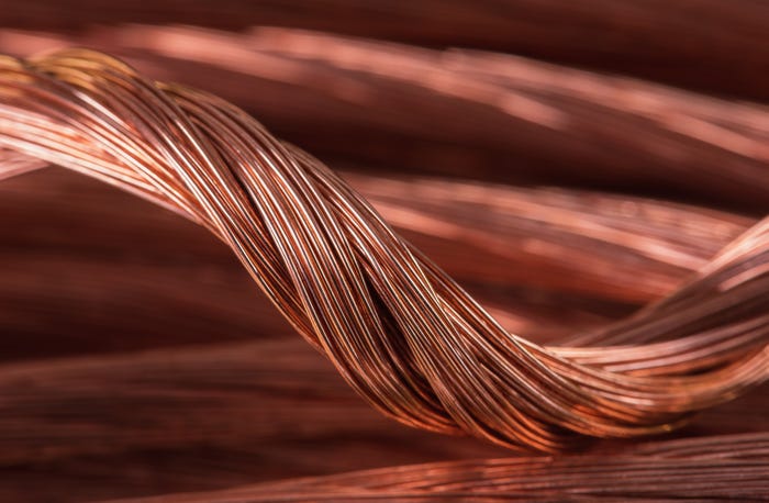
Thanks to its use of high-frequency vibration and pressure to bond metals without melting, ultrasonic welding offers battery producers a promising alternative to traditional welding.


.svg?width=300&auto=webp&quality=80&disable=upscale)


Editors' Choice


Jun 4 - Jun 6, 2024
Jun 4 - Jun 6, 2024
Innovation in automation starts here. Discover and collaborate on automation solutions that are revolutionizing the entire production lifecycle — from design to production to market — and sharpen your competitive edge. ATX South is part of IME South, a six-in-one expo offering the latest insights & solutions spanning medtech, packaging, automation, plastics, design, & processing.
Register NowSign up for the Design News Daily newsletter.