October 21, 2011

Scientists and engineers have created and used microelectromechanical systems (MEMS) since they mastered the fabrication techniques used to transform lab curiosities into sensors, microphones, security devices, engines, and even electromechanical switches for smartphones.
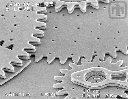
Researchers at the Sandia Corporation have created machines complete with gears and microscopic transmissions, as shown in the photo below. But like all mechanical components, MEMS devices suffer from a variety of failure mechanisms.

The US National Institute of Science and Technology (NIST) recently publicized a new direction for MEMS devices by "machining" diamonds -- the hardest substance known. According to NIST, semiconductor makers hope the diamond-etching techniques will let them develop components for long-lasting micro-machines. In the abstract for a research paper, authors Craig McGray, et al., note:
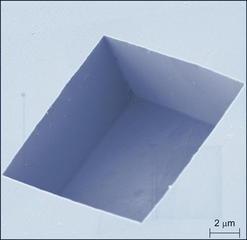
Etching of monocrystalline diamond in oxygen and water vapor at 1100C through small pores in a silicon nitride film produced smooth-walled rectangular cavities. The observed cavities ranged in size from approximately 1μm up to 72μm wide, in each case exhibiting smooth, vertical sidewalls, a flat bottom, and a depth equal to half its width. Cavity boundaries were determined to lie along slow-etching (100) crystallographic planes, suggesting the possibility of a powerful class of techniques for micromachining of diamond.

So far, the NIST researchers have created virtually indestructible nano-rulers, but the etching technology might lead to improvements in MEMS devices because moving parts made of diamond should last much longer than those fabricated from silicon. The inherent cubic-crystal structure of diamonds should also help researchers -- and later, engineers -- create precision structures.
According to NIST, the speed of the etching process depends on the orientation of the diamond crystal. Etching occurs more slowly in the direction of the crystal faces or planes, which can serve as a boundary of sorts where etching would cease as desired. The cavities created at NIST all have smooth vertical sidewalls and a flat bottom.
"We'd like to figure out how to optimize control of this process next," said McGray, "but some of the ways diamond behaved under the conditions we used were unexpected. We plan to explore some of these mysteries while we develop a prototype diamond MEMS device."
I don't relish the idea of having to develop a diamond-etching process with 1100C water vapor formed from hydrogen and oxygen in a reaction chamber, but additional research might uncover other etching and manipulation techniques that lead to diamond-based MEMS. The NIST paper and announcement made no mention of creating structures on the diamond surface, but perhaps deposition of diamond or diamond-like materials could lead to layers of complicated mechanical movements. And even a diamond substrate might improve reliability of present MEMS structures.
About the Author(s)
You May Also Like


