Their small size and low noise make low-dropout regulators ideal for chips' point-of-load duties.
February 1, 2022
Darshil Patel
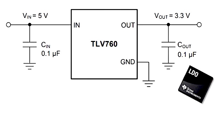
Low dropout (LDO) regulators play a very important role in the power management of an integrated circuit. As a result, mindful designing and selection of LDO circuits become crucial. This article discusses important characteristics and design aspects of low dropout regulators and their practical realization.
As the trend in integrated circuits dictates, supply voltages are decreasing day by day. Furthermore, advanced system on chips (SoCs) employ lower voltage supplied as the feature size of the CMOS fabrication processes decrease consistently. Therefore, to accommodate the need for modern battery-operated electronic devices, demand is growing for highly regulated low-noise power supplies for integrated circuits.
One of the ideal candidates for low-noise DC-DC voltage regulators is low dropout (LDO) regulators. They are small in size, generate low noise, and are ideal for use as point-of-load (POL) regulators that are placed near the target circuit on the chip.
These regulators are simpler and easier to implement than switching converters. The advantages of LDOs over conventional linear regulators, besides low noise and compactness, are that they have a low dropout voltage, high output voltage stability, and low power dissipation.
The dropout voltage mentioned earlier is the difference between input and output voltage. LDOs have a low dropout voltage, and therefore, are more efficient than conventional linear regulators. However, linear regulators like LDOs must dissipate power, and as a result, they are not as efficient as switching regulators. But due to the low dropout voltage, power dissipation in LDOs is significantly less.
LDOs are most commonly used in battery-operated devices. For instance, if a 2.8V LDO is connected to a battery of 4.2V (when fully charged) and the dropout voltage of the LDO is around 200mV, then the LDO can maintain the output voltage of 2.8V ideally even when the battery voltage drops to 3V. In some cases, LDOs are used for post-regulation or filtering. They can be connected at the output of a high-efficiency regulator to provide noise filtering.
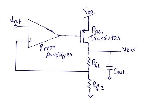
The working of an LDO regulator is quite simple. Generally, conventional LDOs consist of a voltage reference, an error amplifier, a voltage sensing network mostly implemented by a voltage divider, and a PMOS pass transistor.
The pass transistor is controlled by the error amplifier, which compares the reference voltage and the feedback voltage from the output, and amplifies the difference. If the feedback voltage is higher than the reference voltage, the PMOS gate is pulled high, allowing less current to pass, and in turn, decreasing the output voltage.
For the given circuit, the output voltage is given as:

For understanding more about how to design or select every stage of an LDO regulator, it is necessary to have a look at some important LDO specifications or characteristics and get to know how some stages of an LDO design affect them.
Quiescent Current
Quiescent Current (IQ) refers to the current drawn by the LDO when it is active. It is the current flowing through the ground terminal. Therefore, it is also known as ground current or Ignd. Quiescent current is a very important parameter of an LDO as CMOS circuitry mostly operates under a low load.
To understand how significantly IQ affects the efficiency of an LDO, consider a 2.3V battery powering a 1.8V circuit of 2µA of current consumption via an LDO of quiescent current 1µA. This means that even if there is no load attached to the LDO, 1µA of current will flow through the internal circuitry, and some power will be dissipated.
The calculation of total power dissipated by an LDO is straightforward. It is given as:

Plugging in the values, we can see that IQ represents around 69 percent of the total power dissipation. Therefore, for low loads, IQ becomes a crucial design parameter. The IQ depends on the error amplifier and feedback network. To lower the IQ, the current consumption of the error amplifier must be reduced. Moreover, we must make a highly resistive feedback path to ensure less current flows through the ground terminal.
In addition to this, we can also observe that the lower the dropout voltage (Vout-Vin), the lower will be the power dissipation. But when the dropout voltage is too small, it drives the internal circuits in saturation, which will result in a rise in quiescent current.
The demand for lowering the quiescent current can also be seen by the efficiency equation:

Where IIN = IOUT + IQ
In most cases, the output and the input voltage are predetermined. Therefore, the efficiency equation reduces to current efficiency.

So, to achieve maximum efficiency, IQ must be minimum. But there is a tradeoff. Lowering the quiescent current will also reduce the speed of the LDO. Internal nodes of an LDO require a fair amount of current to charge parasitic capacitances when transient occurs.
Lowering the IQ will result in slow charging of these capacitors, and in turn, slower response time. More regarding the speed of an LDO is covered under the Transient Response characteristics.
PSRR (Power Supply Rejection Ratio)
In many cases, LDOs are used to reject supply voltage ripples. These applications demand that the capability of an LDO of suppressing voltage ripples must be high. PSRR is an LDO's capability to suppress input voltage ripples. It is expressed as:

PSRR of an LDO must ideally be very high for all frequencies. To optimize an LDO for high PSRR, it is necessary to understand what factors determine the PSRR.
In the above figure, we can see that the gate voltage of the PMOS varies as the input voltage varies. This variation is because the PMOS tries to maintain a constant voltage difference. Therefore, the supply voltage ripple is attenuated according to the ratio of the output impedance of the LDO and output resistance of the PMOS.
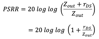
We can observe from the above expression that the output impedance must be reduced to achieve a high PSRR. And it can also be shown that the negative feedback in the regulator does this job of reducing the output impedance effectively.
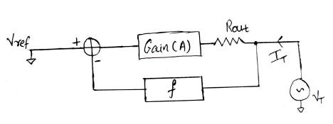
Consider the feedback loop as shown in the figure above. The output impedance can be obtained by calculating VT/IT .
.

Since the gain of the error amplifier is very large, in the order of 100dB, the output impedance is usually small for lower frequencies. But for high frequencies, gain decreases, in turn, lowering the PSRR.
There are various methods to improve PSRR at high frequencies. One simple way is to increase the output capacitance. To see the effect of high output capacitance on PSRR, we plug the value of the output impedance as 1/sCout in the previous equation.

Therefore, we can visualize that a large output capacitor maintains high PSRR even at high frequencies. But a large capacitor can also slow the response time of an LDO. Therefore, to avoid using a large capacitor, one can use an RC filter at the output. But this method increases the dropout voltage of the LDO because of the series resistor.
There are more sophisticated methods to improve the PSRR of an LDO, like adding a charge pump circuit. But the complexity and power dissipation of such LDOs are very high.
Load Regulation and Line Regulation
Load regulation is the capability of an LDO to maintain a stable output voltage under varying load conditions.

Generally, the worst-case variations are calculated when the output current transitions from 0 to maximum.
Line regulation, on the other hand, is the capability of an LDO to maintain a stable output voltage under varying input voltage.

It is trivial to understand that to improve the line regulation, the open-loop gain of the error amplifier must be very high.
Transient Response
During the operation, if an LDO's load changes instantaneously, its operating current changes rapidly, which causes a step-change in the LDO's load current. Ideally, the voltage of the LDO must remain constant under all conditions. However, there is some delay due to the limited operating speed of the LDO. As the load changes, the negative feedback begins noticing the load change. But in the meantime, the drain-source voltage across the PMOS pass transistor changes instantaneously, causing a sudden increase in the output voltage.
The voltage at the output during transients depends on the output impedance and output current change. The feedback cannot track the change in current immediately and reduce the output impedance. Adding a large output capacitor will reduce the output impedance significantly, thus improving the transient response.
But as we know, a large capacitor reduces the speed of an LDO. There is one more specification closely related to speed, namely set-up time. It is the time required by an LDO to settle at an output voltage. The set-up time is affected significantly as the internal capacitors increase.
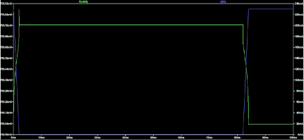
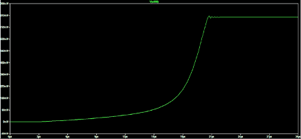
Therefore, as a result of this tradeoff between speed and performance, designers tend to implement a high slew rate error amplifier to improve the set-up time.
As we can see, there are many design aspects for implementing a CMOS LDO regulator. Moreover, besides a careful selection of IQ, dropout voltage, output impedance, and error amplifier design, there are various other aspects regarding stability. Unstable or marginally stable LDOs can run into oscillations and so, compensating the frequency response of LDOs is very critical.
In conclusion, LDOs are at the heart of CMOS power management circuitry, and designing them carefully is very crucial if one wants to achieve low power consumption and reliable power delivery.
Darshil Patel is a passionate electrical engineer. His main interests are in analog circuit design and solid-state physics.
You May Also Like


