Sensor characterization is one of the most important tasks to ensure product development success for load and pressure applications and devices.
December 26, 2020
The first step can often be the most important in any design activity. It certainly is true when engineers work to integrate sensors into their product development process. Here, the first step is the characterization of the sensors. A common example is found in the integration of embedded force and pressure sensors.
Most designers are already familiar with load cell strain gauges and mems sensor technologies. These design choices are not the best for applications that have space or weight constraints as well as power restrictions and cost sensitivity. If the product has such resource constraints, then one should consider using flexible thin-film touch sensors.
Thin-film touch sensors measure compressive forces between nearly any two surfaces. They are ideal for embedding into devices with tight spaces, weight and low power issues that cannot be solved with load cells strain gauges and even MEMS sensors.
Steps
The first step in selecting, designing, and integrating a force or pressure sensor – or any sensor for that matter – is the characterization of the natural phenomena that need to be measured. For example, consider the application of a force sensor to detect and measure the relative changes in a force or applied load.
|
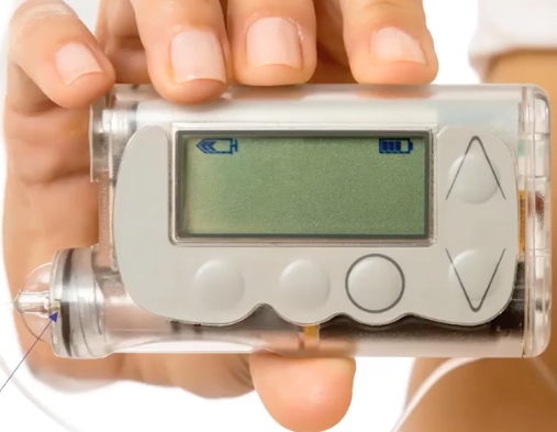
Wearable therapeutic delivery pump. |
Sensor characterization can affect the design, testing, systems integration, and even the manufacturing of a product. Initially, sensor characterization allows you to baseline performance expectations for your application. Later, this same data can be used to troubleshoot unforeseen challenges later in the design phase as well as during prototyping, integration testing, and verification. To demonstrate these points, `consider building a next-generation automated wearable therapeutic delivery pump.
“One of the common challenges these pumps have is the potential for the medication to build up in the delivery system,” explains Ed Haidar, Tekscan Application Engineer, in a webinar video. “To solve this problem, the development team needed a way to monitor relative expansions within the delivery line of the device. The team decided that a force sensing mechanism was required to monitor and measure the change in force from expansions caused by blockage and provide feedback from the device to alert the patient to take action.”
One of the first design constraints was the size as it would be very difficult to fit a load cell into such a tight form factor. Also, the complex embedded electronics required for strain gauges, and even MEM devices could become costly and put a burden on the device's battery life. These constraints were key in the selection of a thin-film sensor for this application. The next activity was to characterize the selected sensor.
Sensor characterization is the process of establishing a fundamental understanding of sensor functionality in a controlled known loading environment. Taking the time to test the sensor with various circuit loading conditions and interface materials is essential in establishing a performance baseline.
Later, if and when unexpected results are observed, the data from an established performance baseline can be used to determine likely causes, isolate the variables, and systematically identify the root cause of observed issues. Without such initial sensor characterization, troubleshooting and debugging of the device could become a costly game of guessing, checking, and then repeating the process.
There are two core questions engineers are looking to answer with sensor characterization explains Haidar. The first one is to determine the fundamental performance of the sensor(s) they plan to use. The second is how the sensor functions with the interfaces, circuits, and materials that are being considered for the application.
When using a force or load sensor, one might be tempted to build their own loading fixture and signal conditioning circuits from scratch. This is not a bad option if the company involved has expertise in that area. If not, it might be more cost-effective to purchase a sensor characterization kit off-the-shelf.
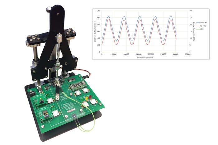
These kits help engineers understand how different force and pressure sensors perform under different circuitry and in controlled loading environments. For example, one such kit from Tekscan includes a desktop loading fixture and an onboard calibrated load cell. This load cell system is required to the characterization process as it provides users with an understanding of sensor capability and performance under known loads. This particular kit includes three interchangeable analog circuit modules sensors and open-source software to control the fixture and record sensor data and a universal power supply.
|
Sample Sensor Characterization Kit |
After acquiring a sensor characterization baseline, the next step is to begin applying loads to the selected force-pressure sensor at the expected force-frequency via the load cell kit or platform. A record of the sensor performance should be kept in a related software program.
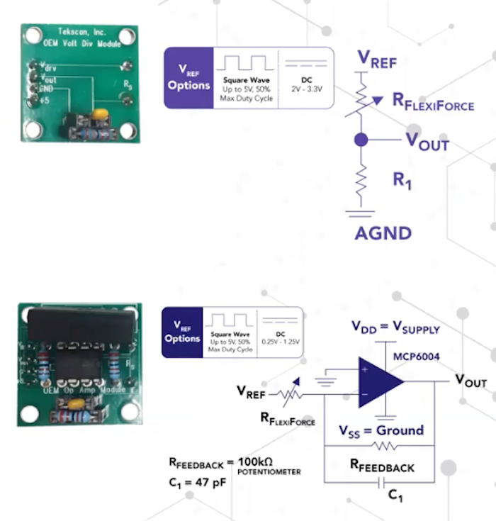
It is not uncommon to note that the sensor responds differently to different circuit configurations. For example, the voltage divider had much less of a linear output curve compared to the inverting op-amp.
|
Sensor output varies with circuit design, e.g. passive voltage divider vs. active op-amp design. |
Once the most appropriate circuit is selected for a given application, the design team tests the sensor-circuit systems with the application's interface materials. Such a test helps to initially size the reference voltage, resistor, and capacitor values within the circuit explained Haidar. Further, the test provides a performance baseline of linearity hysteresis drift and repeatability based on the specific circuit components and interface materials.
After the sensor characterization process is complete, the next step is to create a proof-of-concept, which will help determine whether the sensor can successfully capture its intended measurement with the selected electrical and mechanical configuration. This will be the topic of a follow-on article.
John Blyler is a Design News senior editor, covering the electronics and advanced manufacturing spaces. With a BS in Engineering Physics and an MS in Electrical Engineering, he has years of hardware-software-network systems experience as an editor and engineer within the advanced manufacturing, IoT and semiconductor industries. John has co-authored books related to system engineering and electronics for IEEE, Wiley, and Elsevier.
About the Author(s)
You May Also Like

