Proofs-of-concept and alpha/beta hardware prototyping are essential but challenging activities in product development.
January 19, 2021

After the sensor characterization process is complete, the next step in sensor-based product development is often to create a proof-of-concept. This activity will help determine whether the sensor can successfully capture its intended measurement with the selected electrical and mechanical configurations.
During this phase, the engineering task is to capture the intended measurement using a sensor, electronic signal conditioning, and data communication plus any necessary mechanical structures. The proof-of-concept is a system mock-up to test whether the prototype performs the necessary functions within the established design constraints and requirements.
In our previous example of a wearable therapeutic delivery pump, the proof of concept would use expected interfacing materials and load concentration methods. This would enable the developer to test sensor performance and determine whether the intended measurement or event could be captured.
In sensor systems, vendors will often supply a proof-of-concept prototyping kit that interfaces with the existing embedded printed circuit board (PCB) and operating system. It should include a port to plug in the needed circuit modules plus a way to either monitor feedback from an onboard LED light or from open-source software to allow the live monitoring of force feedback. Another typical requirement for a prototyping kit is to have a programmable and adjustable reference voltage.
A voltage reference is a device that produces a fixed, constant voltage regardless of the load on the device, power supply variations, temperature changes, and the like. Voltage references are used in measurement and control systems, e.g., analog-to-digital converters (ADC) for sensor signal conditioning.
Sometimes, a reference voltage does not provide enough sensitivity to capture a robust measurement, e.g., the reference voltage might be too low for the measurement system to easily detect it. In that case, the reference voltage should be increased, perhaps from 0.5V to 1.0V. A suitable increase in reference voltage will provide increased sensitivity and resolution to reliably-capture a needed measurement.
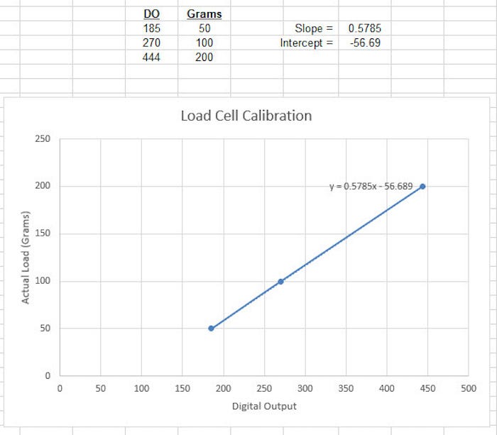
For load cell measurements, a voltage divider is often used to linearly determine a range of loads (see fig). A load concentrator or puck is used to evenly distribute force across the sensing region of a sensor, thus helping to optimize sensor linearity and repeatability. (Image Source: Tekscan, FlexiForce)
|
Linear load cell data captured using open-source software. |
A load concentrator helps direct the force into the sensor's sensing area. It ensures a consistent material interaction – between the load sensor and the load - which optimizes linearity and repeatability. Further, concentrators are also good for protecting the sensor against sheer or abrasive forces that could affect the sensor's sensitivity over time.
Once the proof-of-concept phase has produced acceptable results, the next thing to do is create a prototype. Often, the prototype becomes the initial build of a device. (The other reason to make a prototype is to further flesh out design requirements.) The prototype will be used to reliably calibrate the sensor, identify and deal with sensor variation, and make sure the sensor is robust even for the chosen application.
|
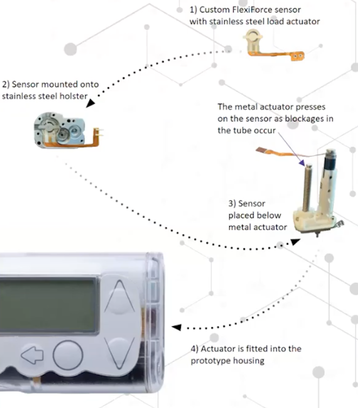
Synthesis of a force sensor inserted in a prototype. |
Let’s return to the wireless medical device example. Basically, the sensor is first fitted with the stainless steel load concentrator, then both are placed within a stainless steel holster and everything is made to fit inside the pump housing. Recall that the prototype consists of a pump housing, fluid delivery tube, embedded sensor, and a voltage divider circuit. It was calibrated using a sensor characterization kit with known loads. (Image Source: Tekscan, FlexiForce)
Once the designer is convinced that this initial (Alpha) prototype is working properly, they move onto a more involved Beta prototype. In the Beta version, the same housing, tube, and HMI components planned for the end-product are used, i.e., digital screen, dials, buttons, etc. Typically, the previous open-source circuit diagrams and layouts of the analog circuit modules are suitable for use in the integrated PCB. Also, the designers incorporated adjustable reference voltage via a digital-to-analog converter (DAC) to accommodate sensor-to-sensor variation.
But as the initial test began with the Beta prototype, a problem occurred. The sensor output was not repeatable when a cyclic load was applied to the tubing sensor. Initially, the developers thought the sensor was malfunctioning or didn’t have the needed range. But by comparing the data collected during earlier characterization to the data collected from the prototype, the developers were able to isolate the variables that could cause the deviation. They determined that the sensor was actually doing its job and it was the plastic tubing that was causing the issue.
It turned out the tubing was configured in such a way that it could slightly move off the sensor during use, which was the likely cause of the erratic data. To solve this problem, the developers modified the assembly that held the tubing in place so that it would remain in contact with the sensor. This proved to be a much better mechanical setup.
The next step was to create the software application and field test the device. This will be covered in a follow-up article.
John Blyler is a Design News senior editor, covering the electronics and advanced manufacturing spaces. With a BS in Engineering Physics and an MS in Electrical Engineering, he has years of hardware-software-network systems experience as an editor and engineer within the advanced manufacturing, IoT and semiconductor industries. John has co-authored books related to system engineering and electronics for IEEE, Wiley, and Elsevier.
About the Author(s)
You May Also Like


