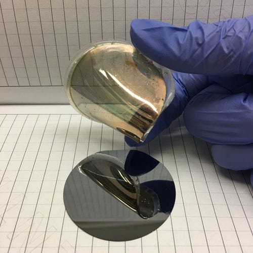
Researchers at Missouri University of Science and Technology have developed a way to “grow” thin layers of gold on single crystal wafers of silicon, then remove the gold foils and use them as substrates on which to grow other electronic materials.
May 26, 2017
They say all that glitters is not gold. In the future, however, it may well be the reverse: even some things that don’t glitter—like a smartphone that can wrap around a person’s wrist--could very well be made from the precious metal, thanks to a new method devised by researchers to develop electronic materials from gold.
Researchers at Missouri University of Science and Technology (S&T) have developed a way to “grow” thin layers of gold on single crystal wafers of silicon, then remove the gold foils and use them as substrates on which to grow other electronic materials. The team—led by Jay A. Switzer, a chemistry and materials science and engineering professor at the university—said their method could significantly advance the development of wearable or flexible technology by improving the versatility of these types of electronics.
“To expand the palette of electronic materials beyond silicon, an inexpensive source of highly ordered material is needed that can serve as an inert substrate for the epitaxial growth of grain boundary-free semiconductors, optical materials, and superconductors,” Switzer explained to Design News. “We show that wafer-size transparent and flexible single-crystal foils of gold can be produced by a simple and inexpensive lift-off procedure using single-crystal silicon as the template for electrochemical epitaxial growth. These single-crystal gold foils offer the order of traditional semiconductors such as silicon wafers without the constraint of a rigid substrate.”
Switzer said the development of wearable technology is currently limited because most researchers are working with polymer substrates, or substrates made up of multiple crystals. Because of these multiple crystals, the substrates have what are called grain boundaries, which can greatly limit the performance of an electronic device, he said.
“Say you’re making a solar cell or an LED,” Switzer said. “In a semiconductor, you have electrons and you have holes, which are the opposite of electrons. They can combine at grain boundaries and give off heat. And then you end up losing the light that you get out of an LED, or the current or voltage that you might get out of a solar cell.”
|
An example of a gold foil peeled from single crystal silicon. Researchers at Missouri University of Science and Technology (S&T) have developed a way to “grow” thin layers of gold on single crystal wafers of silicon, then remove the gold foils and use them as substrates on which to grow other electronic materials. The team said their method could significantly advance the development of wearable or flexible technology by improving the versatility of these types of electronics. (Source: Naveen Mahenderkar/Science/Missouri University of Science and Technology) |
While silicon comprises most electronics on the market because it’s relatively cheap and works well, it’s also comprised of a single crystal with perfectly aligned atoms, which makes it typically inflexible, he said.
The difference in what Switzer and his team developed in their new work is that they started with single crystal silicon and then grew gold foils on it, which allowed them to keep the high order of silicon on the foil. At the same time, because the foil is gold, it also led to the development of a material that also is highly durable and flexible.
Switzer said it was the inertness of gold that was key to making it so well-suited for the research, which depended on different types of fabrication methods to develop.
“We chose gold because it is inert, and can serve as the substrate for growing a wide variety of materials,” he said. “The inertness of gold is important, because it allows the deposition of films by solution methods such as electrodeposition, hydrothermal processing, and chemical bath deposition.”
The team’s work will enable the production of electronic devices that are flexible yet lack grain boundaries, so they should be more efficient than what’s currently being produced for flexible and wearable technology, Switzer said. Researchers published a paper describing their work in the journal Science.
While gold is indeed more expensive than silicon, the foils developed by the researchers are very thin--on the nanometer scale, Switzer said. This means they won’t be very expensive to produce. Moreover, nearly anyone can produce them because there is no need for high-vacuum processing, he said.
“This is something that I think a lot of people who are interested in working with highly ordered materials like single crystals would appreciate making really easily,” Switzer said. “Besides making flexible devices, it’s just going to open up a field for anybody who wants to work with single crystals.”
About the Author(s)
You May Also Like


