December 29, 2014

Consumers today expect their electronic devices to have simple, intuitive, and visually attractive interfaces. Nested menus with pushbuttons are being replaced by resistive or capacitive touch displays on everyday products such as washing machines, thermostats, and car dashboards. For engineers chartered with building these embedded devices, component selection and board design have always been a challenge. The constraints of traditional microprocessor (MPU) system architecture have bound them to using Flash memory for code storage and DRAM for code execution and graphics buffering.
But there is a new paradigm available for embedded system designers that holds the promise of disrupting this traditional design pattern. With the availability of abundant on-chip SRAM within an MPU today, coupled with the ability to execute code highly efficiently directly from Flash, design engineers can forgo the use of DRAM in their MPU systems. By doing so, they are able to simplify board design, lower their bill of materials (BOM) cost, and reduce system-wide power consumption, all while increasing performance.
Simplify PCB Design while Reducing System Cost and Power
According to a 2013 UBM Embedded Market Survey, roughly 30% of the embedded design cycle is focused on simulation, testing, and debugging. Fortunately, for designers of microcontroller (MCU)-based systems, connecting to, simulating, testing, and debugging DDR SDRAM interfaces is not a challenge they need to face. MCUs contain on-chip Flash (4 MB and higher in some cases) that allows for code storage and execution from within a single device. Unfortunately, MCUs are not suitable for high-end human-machine interface (HMI) applications since they do not tend to clock higher than a few hundred Dhrystone million instructions per second (DMIPS) or handle display resolutions much above WQVGA (480 x 272). MPUs, by contrast, can easily process WXGA (1280 x 800) resolution and above. Thus, for systems that demand application-class performance and highly polished graphical interfaces, an MPU is usually needed. MPU architecture and peripheral sets are more sophisticated than that of MCUs. However, MPUs lack on-chip Flash and usually have only a modest amount of SRAM. These limitations necessitate code storage in external Flash and run-time execution from DRAM.
Numerous design considerations and physical connections are required to hook up a DDR SDRAM memory to an MPU. For instance, a typical 1 GB 16 bit DDR3 SDRAM will consume 40 or more device pins (for data, address and control signals) and will require additional power supplies. This often leaves the MPU I/O-bound and the PCB plagued by routing congestion. To cleanly disseminate all of the requisite power rails around the PCB, designers will often mount power management ICs (PMICs) to the board. While this reduces the number of components, it burns PCB real estate and consumes more power, which compounds the overall challenge of PCB design.
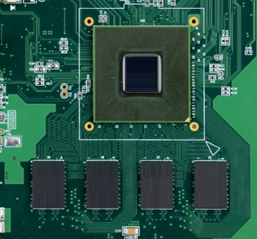
To complicate matters, the quoted performance specifications of a DDR memory can only be achieved if its data and clock traces are length-matched precisely on the PCB. This is because DDR SDRAM devices use a source synchronous interface topology, where the clock and data must be sent to and from the MPU together with minimal skew – typically 10s of picoseconds max. The routing complexity is illustrated in Figure 1. Near-end and/or far-end termination resistors are also required for impedance matching to ensure proper switching characteristics. Failure to properly design and lay out the PCB with signal integrity and performance considerations in mind often results in boards that are electrically noisy and that must be re-spun.

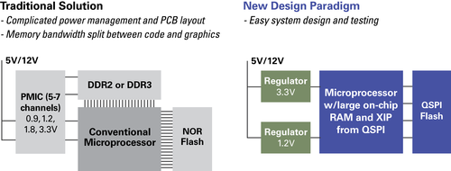
Fortunately, MPU designs no longer have to be bound by the challenges inherent to the traditional three-chip-solution of MPU, Flash, and DRAM. With MPUs that offer up to 10 MB of on-chip SRAM today, an application’s entire software stack (libraries, operating system, and source code) plus graphics buffers can be contained completely within the same device. For designs with a larger code-base, execution-in-place (XIP) is also possible from inexpensive quad serial (QSPI) Flash memory. This offers the added advantage of faster start-up because code does not need to be loaded into SRAM. The multilayer predictive caching and out-of-order execution capabilities of modern processors, like the ARM Cortex-A9, facilitate high-performance code execution from Flash. The simplicity of this new design paradigm is contrasted to the traditional solution in Figure 2. Designers who employ high availability on-chip memory devices will enjoy the numerous benefits that stem from fewer board components, including simplified board design, reduced BOM cost, and lower power.

Increase System Performance
In traditional MPU system design, DRAM bandwidth must be split between code execution and graphics frame buffering. This creates an unavoidable memory-access bottleneck, which can adversely affect touch display appearance and responsiveness. This is because in a graphics-rendering device, the off-chip bus arbiter inside the memory controller must time-slice these two equally important activities. When you buffer up a WXGA graphic frame, for example, you impose a severe bottleneck on your code execution architecture because the memory is busy buffering data. Conversely, when a CPU is executing code that cannot be interrupted, like in a tight loop or within a critical function, the data connection to the frame buffer is temporarily halted. This can adversely impact the touch display’s performance, delaying touch response and contributing visual artifacts.
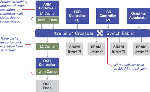
Even if you lay out your board cleanly enough to achieve the maximum theoretical clock rates of the DDR SDRAM memory, there are some fundamental limitations that cannot be avoided in a three-chip architecture. For example, read and write latency is incurred upon every memory access. This latency is magnified when the memory controller opens, closes, and switches banks inside the DRAM in order to address its full memory span. In fact, the more non-sequential the memory accesses, the more bank switching is needed and the greater the performance penalty. Furthermore, an external memory typically only allows for monatomic access; whereas on-chip memory can be broken into multiple banks or pages and connected to a wide, simultaneous access multi-mastering bus (or “switch fabric”).
MPUs are available (see Figure 3) that offer an appropriate memory bus architecture, allowing for x4 parallel accesses and providing a maximum theoretical bandwidth of 8.5GB/s (i.e. 128bits x 133MHz / 8bits/byte x 4). Compare this to a 16-bit wide 400 MHz (i.e. 800 Mbps) DDR3 memory with a theoretical maximum bandwidth of 1.6 GB/s (i.e. 16bits x 800Mbps / 8bits/byte). From a sheer memory bandwidth perspective, this is greater than a 5x difference.

Today, there appears to be an answer to some of engineering management’s toughest questions: How can we lower our system development budget and cost of goods sold (COGS)? How can we get to market faster while meeting the tight power constraints of today’s energy-conscious original equipment manufacturers (OEMs)? Finally, how can we provide enough memory bandwidth and graphics processing horsepower to meet the challenges of modern HMI design? With an MPU that includes abundant on-chip SRAM and the ability to execute code in-place efficiently from low-cost serial Flash memory, designers clearly have a new option. Ultimately, it is the end customer who enjoys its benefits the most -- through better, more visually appealing products and improved user experience.
David Olsen is staff product marketing manager for Renesas Electronics America
Design engineers and professionals, the West Coast's most important design, innovation, and manufacturing event, Pacific Design & Manufacturing, is taking place in Anaheim, Feb. 10-12, 2015. A Design News event, Pacific Design & Manufacturing is your chance to meet qualified suppliers, get hands-on access to the latest technologies, be informed from a world-class conference program, and expand your network. (You might even meet a Design News editor.) Learn more about Pacific Design & Manufacturing here.
About the Author(s)
You May Also Like


